
Abstract
It is shown, by calculations calibrated against the authors' recent experimental data, that an eye-safe wavelength range InGaAsP/InP high pulsed power laser design using a bulk active layer, which has a large refractive index step with respect to the optical confinement layer and is located close to the p-cladding, can provide substantial performance improvement compared to the best results achieved so far for this operating regime and wavelength. The dependence of the laser performance on the design parameters such as the thicknesses of the active layer and the waveguide, as well as the cavity length, are analysed. It is shown that the relatively thick bulk active layer in such InGaAsP/InP lasers allows the use of short cavity lengths (∼1 mm or even shorter), for achieving high pulsed power while maintaining a low p-cladding series resistance (making for high efficiency) and a narrow far field (making for high brightness). A single-asymmetry structure with the asymmetric active layer location but symmetric optical confinement layer/cladding refractive index steps gives performance only marginally inferior to that of a double-asymmetric one including asymmetric refractive index steps.
Export citation and abstract BibTeX RIS

Original content from this work may be used under the terms of the Creative Commons Attribution 4.0 license. Any further distribution of this work must maintain attribution to the author(s) and the title of the work, journal citation and DOI.
1. Introduction
High power broad area pulsed diode lasers operating in the eye-safe spectral range, i.e. within the wavelength range from 1400 to 1700 nm, find applications ranging from medical instrumentation to range finding/LIDAR systems [1]. There has been much work in the recent years aimed at improving their performance (power and brightness); several device designs have been proposed. The general strategy in designing high-power semiconductor lasers is to ensure high output efficiency for all operating currents. This, in turn, requires that the internal losses in the lasers are engineered to be as low as possible [2] and to increase as little as possible at high operating currents. Implementation of this strategy for eye-safe range lasers is influenced by the very high value of the free hole (intervalence band) absorption cross-section (>30 times greater than the free-electron one). Thus, for lasers in this wavelength range it is particularly important to minimise the overlap of the waveguide mode with any heavily p-doped regions in the laser structure (primarily the p-cladding), and also to minimise the accumulation of holes at high carrier densities in the laser waveguide. In the absence of heating (i.e. under pulsed operation), the main mechanism of such carrier accumulation is the (unavoidable) spatially inhomogeneous carrier accumulation in the Optical Confinement Layer (OCL) of large optical cavity (LOC) lasers due to current flow. A detailed theory of this effect was developed in our papers [3] (for an undoped or very weakly doped structure) and [4] (for a doped structure). It has been shown that by far the most efficient way to minimise the increase in the internal losses at high injection levels due to the inhomogeneous hole accumulation is to minimise the physical thickness of the p-OCL, that is, the side of the OCL that is adjacent to the p-cladding. The most successful designs of high-power eye-safe wavelength lasers do indeed all have thin p-OCL layers [5–13]. The two designs of high-power quasi-continuous-wave lasers, at any wavelength, most widely used currently are the ultranarrow waveguide [5–8] and the broad asymmetric waveguide [12–17] designs. Both have been applied for the eye safe wavelength range [5–8, 12, 13]. Both of these designs, in addition to the high raw power, also allow for a single, broad transverse mode, leading to a relatively narrow far field and consequently high brightness. In the ultranarrow waveguide, this broad near field distribution is due to weak waveguiding with strong mode penetration into the claddings, which necessitates graded p-doping of the p-claddings [7, 8], by necessity compromising both the built-in optical losses (hence power) and the electrical resistance (hence efficiency) of the laser. In strongly asymmetric Large Optical Cavity waveguides, the single broad mode is achieved by using asymmetric refractive index steps at the n-OCL/n-cladding and p-OCL/p-cladding interfaces in addition to the asymmetry of the active layer position, resulting in double asymmetry or, in the most recent implementation, triple asymmetry to maximise the mode overlap with the active layer (the optical confinement factor Г [17]). This last step was made necessary by the fact that nearly all high-power laser structures used so far have used active layers consisting of only a few (1–3) Quantum Wells (QWs). In such structures, the active layer itself tends to have very little effect on the waveguide properties. In lasers working at the wavelength of around 1 µm (and in any structures involving InGaAs ternary layers grown on a GaAs substrate), using a thicker active layer is difficult for technological reasons. For lattice matched structures, e.g. GaAs/AlGaAs system and the eye-safe wavelength InGaAsP/InP lasers, there is no such technological limitation. In our work, double-asymmetric designs with a bulk active layer in a GaAs/AlGaAs λ ≈ 0.85 µm laser and, later, in an InGaAsP/InP λ ≈ 1.5 µm device, have been proposed [18, 19] and realised [12, 13, 20] in lasers operating in the the gain-switched [18, 20] and quasi-CW pulsed [12, 13, 19] regime. The results compared favourably with the best published results, with considerable scope for further optimisation. In [18, 20], the relatively broad (d= 800 Å) active layer still did not substantially affect the waveguide properties due to the relatively small refractive index contrast (Δnact ∼0.1) between it and the waveguide. The later work on the InGaAsP/InP lasers[12, 13] used a material composition that provided a higher refractive index contrast (Δnact∼ 0.3), so the active layer itself (d = 600 Å) noticeably affected the mode profile, with the mode peak being attracted to the active layer position thus increasing the value of Г. Pulsed power outputs of ≈18 W, comparable to the best results reported in the literature, were achieved in lasers with stripes 90 µm wide and cavity lengths of 1 and 2 mm, at a current amplitude of 80 A and a pumping pulse duration of ≈60 ns. We believe the results were limited to a substantial extent by the injection efficiency (≈0.7–0.8) and, in the case of lasers 1 mm long, the mounting of the laser hence its thermal resistance.
Here, we present a more systematic theoretical study of high-power laser design with bulk active layers with substantial waveguiding effect, and show that they offer new paths in laser design and optimisation.
2. Structure
As discussed in the Introduction, the distance between the active layer and p-cladding needs to be small to avoid carrier accumulation at high injection levels. Minimising the modal overlap requires a substantial refractive index step at the p-OCL/p-cladding interface. Following the earlier work, we shall consider designs with thick waveguide layers, partly to help minimise the mode overlap with the p-cladding and partly to ensure the broad fundamental mode distribution (as shown in figure 1) in order to ensure a narrow far field and high brightness. Thus the parameters that will be fixed in the studies below are the two refractive index steps (Δnact≈ 0.27, and Δnp≈ 0.064 as in [12]), and the thicknesses of n-OCL layer (ln-OCL = 1.8 µm as in [12] or 2.8 µm as in [19]) and the p-OCL layer (lp-OCL = 0.15 µm, as in [12]). The parameters that can be varied are the refractive index step at the n-OCL/n-cladding interface Δnn and the width of the active layer d.
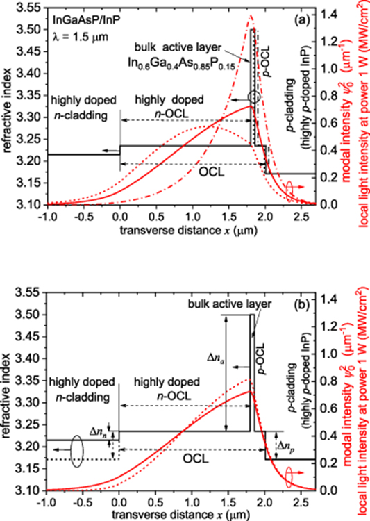
Figure 1. Schematic of the laser structure and the waveguide mode intensity distributions for waveguides with: (a) the active layer thicknesses d= 600 Å (solid), 400 Å (dashed), and 1000 Å (dash-dotted), (b) d= 600 Å and symmetric (dashed lines) and asymmetric (solid lines) refractive index steps at the OCL/cladding interfaces. Stripe width w = 100 µm.
Download figure:
Standard image High-resolution imageFigure 1(a) shows the effect of the active layer width on the modal properties of the laser. It shows the refractive index profiles and the corresponding modal profiles for a family of laser designs including that used in the experiment [12], with the active layer thickness d= 600 Å, and also with a thinner (d= 400 Å) and thicker (d= 1000 Å = 0.1 µm) bulk active layers. Apart from the value of d, the waveguide designs are identical: in addition to the fixed parameters mentioned above, they are all double-asymmetric waveguide structures with the refractive index contrast at the n-OCL/n-cladding interface of Δnn≈ 0.02, approximately three times smaller than Δnp. Note that in practice, the n-cladding has a finite width which we take to be of 3 µm as in the experimental structures of [12], so that at x= −3 µm, there is another refractive index step to the InP value, not shown in the figure but taken into account in calculations. It has virtually no effect on the properties of the fundamental mode but affects the modal selectivity for small values of d. As will be shown below, all three structures ensure reliable selection of the fundamental transverse mode.
Figure 1(b) illustrates the effect of the refractive index step asymmetry on the modal properties, by presenting the modal distribution of the 'reference' asymmetric waveguide (the same as in the experiment of [12, 13] and figure 1(a)) alongside a waveguide identical to it, but with symmetric refractive index steps Δnn = Δnp =0.064.
As seen in figure 1(a), the guiding properties of the active layer are quite important for the waveguiding in the laser: in the structure with d= 400 Å, the modal peak is relatively far from the active layer, whereas the active layer with d= 600 Å attracts the modal peak, and the value of d= 1000 Å to a significant extent localises the mode at the active layer. This is reflected in the strong and markedly nonlinear increase in the confinement factor Г of the fundamental mode with the active layer thickness d, as illustrated in figure 2. For comparison, the figure also shows the highest value of Г for a non-fundamental mode (which for the waveguide of figure 1(a) is the mode 1 for d> 400–450 Å and the mode 2, which only exists because of the finite thickness of the n-cladding, for smaller d values), whose dependence on d is much weaker. The difference in the confinement factor values for the fundamental and higher order mode largely ensures good modal selectivity in both the symmetric and asymmetric index step waveguide, at least for d> 400–1000 Å.
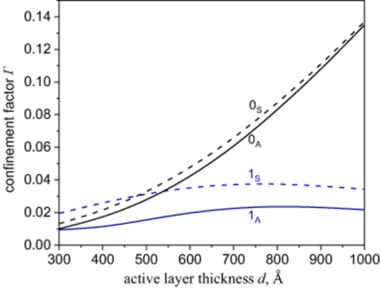
Figure 2. Confinement factor Г as function of the active layer thickness for the fundamental mode (0 S,0A) and the higher order mode nearest to excitation (1 S,1A) for a waveguide with symmetric (dashed lines 0 S,1 S) and asymmetric (solid lines 0A,1A) refractive index steps at the OCL/cladding interfaces. The waveguide parameters as in figure 1.
Download figure:
Standard image High-resolution imageFigure 1(b) shows that the symmetry or asymmetry of the refractive index steps at the OCL/cladding interfaces has a rather modest effect on the fundamental mode for large enough values of d (>500 Å or so in our case). This is confirmed by figure 2, showing that the confinement factors in the structure with the symmetric Δnn = Δnp becomes progressively closer to that for Δnn <Δnp as d increases; for d = 1000 Å, when the waveguiding is defined to a substantial extent by the active layer rather than the OCL, the values of Г for the two structures are almost identical.
The asymmetric structure provides a more pronounced advantage in the fundamental order mode confinement factor compared to that of the higher order modes, however for large enough values of d this is likely to be superfluous—the modal discrimination is very strong in any case.
3. Analysis of laser performance
In this paper, we consider pulsed (quasi-CW) operating regime, with the injection current pulse short enough to not cause laser heating, as is the case in LIDAR applications (e.g. 60 ns long pulses as used our previous work [12, 13] should satisfy this condition given modest repetition rates and good quality laser mounting), so room temperature operation is assumed throughout. For evaluating the threshold and power characteristics of the laser, as in [12, 13, 19], we can then use the experimentally validated [21] linear approximation for the peak gain dependence on the carrier density:  ; the gain cross-section σg and the transparency carrier density Ntr were taken from that paper as in [12, 13, 19]. The free electron (
 ) and hole (
 ) absorption cross-sections in the active layer (and the OCL) were also the same as in [12, 13, 19], namely
  = 5 × 10⁻¹⁹ cm2 [22],
  =4 × 10⁻¹⁷ cm2 [23, 24]. Then, the threshold carrier density of the laser is estimated (neglecting the loss due to carrier accumulation in the OCL, which is very weak at threshold) using the simple expression
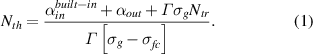
Here,  , and the built-in losses
  are mainly formed by the free hole absorption in the moderately doped p-OCL and highly doped p-cladding. The result is shown in figure 3 as function of the active layer thickness d, with the outcoupling losses
  calculated for the facet reflectivities of RHR= 0.95 and RAR= 0.05 and the cavity length values of L= 0.5 mm, 1 mm, and 2 mm. The values of Nth, as can be expected, are higher for the shorter cavity, making for some compromise in the threshold current compared to the longer laser, however for large enough d, the absolute values of Nth are still not high, and as will be shown later, this slightly higher threshold current is justified for keeping good output efficiency at high injection levels.

Figure 3. Active layer carrier densities and active layer losses at threshold as functions of the active layer thickness d for waveguides with symmetric (dashed lines) and asymmetric (solid lines) refractive index steps at the OCL/cladding interfaces. The waveguide parameters as in figure 1.
Download figure:
Standard image High-resolution imageAlso shown in figure 3, as function of d, is the contribution  of the free-carrier absorption in the active layer to the internal losses in the laser at threshold. As can be expected, Nth decreases noticeably with the thickness of the active layer d, though
  increases somewhat with d due to increase in Г. For large d values, the values of Nth for the lasers with the symmetric (Δnn =Δnp) and asymmetric (Δnn < Δnp) refractive index steps are very close due to similar Г values. We have also compared the values of the threshold gain
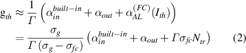
for the fundamental and higher order modes, making sure that excellent modal selectivity is indeed achieved in both structures, e.g. for d= 600 Å as in [12], the value of gth for the asymmetric-step waveguide is ≈580 cm−1 and the one for the symmetric-step waveguide is and ≈530 cm−1, while for the first order mode, they would be ≈1100 cm−1 and ≈730 cm−1 respectively.
Thus the presence of the relatively thick active layer, with a large refractive index step Δna, in a LOC waveguide, firstly, allows reliable selection of the fundamental order mode even in a waveguide with Δnn =Δnp, and, secondly, makes for relatively low threshold carrier density compared to lasers with thinner active layers. It also allows us to confidently expect thermal spillout of carriers into the waveguide and the p-cladding to be negligible in a broad range of currents, both at room temperature and at moderately elevated temperatures, particularly since a large contrast Δna goes along with a deep potential well. This, in turn, removes a potential source of IVBA loss, particularly important in long-wavelength lasers as mentioned above, as well as suppressing the threat of current leakage. Thus the relatively low threshold carrier density is what allows the use of samples as short as 1 mm for high-power pulsed lasers, operating high above threshold.
As in previous work [12, 13, 19], the total internal absorption in the laser as function of the current I and the power P(I) was calculated as the sum of several contributions
This includes the built-in optical losses  discussed above, the free hole absorption in the active layer
  , the loss
  due to current-induced carrier accumulation in the OCL (in the current design with active layer located very near the p-cladding, this means mainly in the n-OCL), and the direct
  and indirect
  contributions of the two-photon absorption (TPA) [19]. It is worth noting here that the TPA coefficient β2,OCL= 6 × 10⁻⁸ cm W−1 of the InGaAsP OCL material significantly exceeds the corresponding value in AlGaAs materials, making the TPA effect particularly important to consider in eye-safe wavelength range lasers.
All the contributions to the internal loss coefficients were calculated as in [12, 13, 19]; the stripe width for recalculating the current values into current densities was w = 100 µm.
As in earlier work, the loss was calculated self-consistently alongside the light-current characteristics P(I), found from the transcendental equation
Here, as in previous work, the effective threshold current  is the current expended on creating the active layer carrier density necessary for the gain to compensate the total losses
  at the given current value I, and the injection efficiency is taken as
  as in [19]. Unlike the as-cleaved lasers of [12, 13], here we are considering lasers with asymmetric AR/HR coated facets; however the relatively short cavity lengths and the relatively high AR coating reflectance make it possible to use a lumped model with no modification to the equation (4); the LSHB coefficient [25] for this laser design is very close to one.
Figure 4(a) shows the individual contributions to the internal optical losses as well as the resultant  value, as functions of current I for a 1 mm long laser cavity. The total losses grow from 9 to 18 cm−1 over the interval of currents shown. Both the initial value of
  and the range of its increase with current are noticeably higher than in the case of a 2 mm long laser with the same parameters of the waveguide and doping levels. This is mainly because of the higher active layer carrier density affecting the losses, and also because of the TPA-related contribution to
  (mainly the indirect one
  ) which scales with power P as P2 and is thus stronger for the 1 mm long laser with its higher power output (see figure 5).
Figure 4. (a) Calculated output power, total internal loss and its individual components as functions of current:  (1),
(1),  (2),
(2),  (3),
(3),  (4),
(4),  (5). L= 1 mm, (b) total loss and output efficiency for three lengths of the resonator as functions of current. Asymmetric refractive index steps at the OCL/cladding interfaces (Δnn<Δnp), stripe width w = 100 μm, and d = 600 Å used for calculating both figures. The rest of the waveguide parameters as in figure 1.
Download figure:
Standard image High-resolution image
Figure 5. Calculated output power for the structures with symmetric (solid lines) and asymmetric (dashed lines) refractive index steps at the OCL-cladding interfaces, for different values of the cavity length L and n-OCL thickness ln-OCL and waveguides with symmetric (dashed lines) and asymmetric (solid lines) refractive index steps at the OCL/cladding interfaces. The active layer thickness is d= 600 Å for ln-OCL =1.8 μm and d= 700 Å for ln-OCL = 2.8 μm, the stripe width w = 100 μm. The rest of the waveguide parameters as in figure 1.
Download figure:
Standard image High-resolution image
As in [12, 13], the current-induced carrier contribution  is strongly suppressed: the p-OCL contribution mainly by the asymmetric active layer position and the n-OCL contribution by the high n-OCL doping (substantially higher than in [12]). The direct effect of TPA is also very weak, as in [12]. This leaves the indirect effect
  as the main reason of the increase in
  with current in this material and laser design, though this effect, too, is partly suppressed by the recombination of the TPA-generated carriers in the highly doped n-OCL.
Figure 4(b) shows the total internal loss and the output efficiency  as functions of current for three cavity length values. It is seen that, despite the higher internal losses, the shorter laser cavities still show a markedly higher output efficiency than the longer ones, due to the higher value of the outcoupling losses
  . This is a direct result of the minimisation of the losses due to the carrier accumulation
  in our laser design—to a good accuracy, this component of internal absorption is proportional to the current density
  and is therefore substantially higher in shorter lasers for the same total current value compared to the longer ones. In the current laser design, given the small absolute value of
  , this does not cause a problem, but in a design with a more symmetric active layer position where
  is the dominant loss mechanism, the effect could be drastic, causing the output power of shorter lasers to saturate and dip below that of longer lasers at sufficiently high injection levels.
Figure 5 shows the calculated light-current curves for lasers with three cavity lengths (L= 0.5 mm, 1 mm and L= 2 mm) as in figure 4(b), for two thicknesses of the n-OCL (ln-OCL = 1.8 µm as in [12] and 2.8 µm as in [19]), and for the two cases of refractive index steps (Δnn <Δnp and Δnn =Δnp).
The figure has two noteworthy features. Firstly, as could be expected from figure 4(b), the lasers with shorter cavities give higher output powers at high injection levels, despite the higher total losses. Secondly, in the current design, in which the waveguiding is to a substantial extent provided by the active layer itself due to large d and Δna, the effect of the symmetry or asymmetry of Δnn and Δnp is rather small. The double-asymmetric structure with Δnn <Δnp still gives a higher output than the single-asymmetric one with Δnn =Δnp, but only slightly (note that the far field is also somewhat narrower for the structure with Δnn <Δnp than for Δnn =Δnp, e.g. for ln-OCL = 1.8 µm, the predicted far-field full-widths at half—maximum being 24 and 30 degrees respectively).
The power values predicted, for the stripe width considered (w= 100 µm), the room temperature operation, and high injection level (I∼ 100 A), promise a substantial step forward compared to the best published results [9–11]. Note also that the doping level of the all p-claddings in the lasers considered here is 2 × 1018 cm−3, much higher than in [9, 10] (no data on doping was given in [11]) which is expected to help improve, not just the raw power as discussed above, but also the series resistance and hence the wall-plug efficiency of the laser.
4. Discussion and conclusions
As mentioned above, the use of short cavities, allowing the high value of  and hence high output power despite the relatively high internal losses, is made possible by the thick active layer and the large bandgap (and correspondingly refractive index) steps between the active layer and the OCL. The latter, as discussed above, leads to substantial values of Г, which reduces the threshold carrier density value (equation (1), figure 3) and hence helps suppressing both an increase in
  (important due to the high Auger recombination in InGaAsP materials) and degradation of ηi through possible carrier/current leakage into the p-cladding. At the same time, the broad OCL helps maintain a relatively broad modal distribution (figure 1) and therefore good far field parameters and modest TPA effects. Unfortunately, it does not therefore appear possible to use the design proposed here for shorter-wavelength lasers operating at λ ≈ 1 µm. To begin with, realising thick active layers in the InGaAs/GaAs/AlGaAs system most commonly employed at that range of wavelengths is technologically highly problematic as discussed in the Introduction. Secondly, although in principle it is possible to design an InGaAsP/InP structure for that wavelength range, the active layer could be broad but it would not be possible to achieve sufficiently large bandgap and refractive index steps.
We can however note in passing that a design strategy similar to the one used here—the use of bulk active layers—is also employed in a totally different class of lasers where cavity losses are high, namely λ ≈ 1.5 µm semiconductor nanolasers [26, 27]. Further broadening the active layer and making its position in the large optical cavity asymmetric may thus prove beneficial for those lasers as well.
Note finally that the designs of lasers used in [12] and particularly [13] were quite similar to some of those presented here. We believe the reasons why the power levels achieved experimentally, while quite respectable, were not as high as those predicted here were, firstly, the injection efficiency value ηi= 0.7–0.8 (we assume ηi = 1 here); secondly, the narrower stripes; thirdly, the nature of laser mounting that could not eliminate some degree of residual heating of L = 1 mm samples; and, finally, the as-cleaved structure which gives a slightly smaller value of  . None of these limitations are fundamental or unavoidable. The preliminary experimental results of [13] still showed that 1 mm long λ = 1.5 µm lasers with bulk active layers (and designed to suppress the absorption due to nonuniform carrier distribution in the OCL) give higher power output at high injection level than 2 mm long ones, in agreement with the theory presented here.
As mentioned above, in addition to making for good series resistance and hence potentially contributing to a high wall-plug efficiency the use of highly-doped p-claddings in the current design also decreases the rate of electron spill-out from the active layer to the p-cladding [28–30] meaning that the structures considered may prove relatively tolerant to temperature increase and thus possibly advantageous for CW as well as pulsed operation.
To conclude, the structures proposed and analysed are predicted to offer a significant advantage over existing designs for high optical power generation in the pulsed regime in the eye safe wavelength range. The use of a relatively thick, bulk active layer with a large bandgap and hence refractive index contrast with respect to the OCL makes it possible to use short optical cavities effectively, improving the output efficiency and hence power while maintaining a small series resistance of the p-cladding layer, helping maximise the total efficiency. It also almost eliminates the need for double and triple asymmetry, required at shorter-wavelength lasers, since waveguiding properties of the active layer itself both provide the asymmetry of the waveguide mode with low penetration into the p-cladding, and enable a high value of the optical confinement factor.
Acknowledgments
This work was supported by the Academy of Finland, Centre of Excellence in Laser Scanning Research under contract 317144.