
Abstract
Transition metal dichalcogenides (TMDs) have received immense research interest in particular for their outstanding electrochemical and optoelectrical properties. Lately, chemical gas sensor applications of TMDs have been recognized as well owing to the low operating temperatures of devices, which is a great advantage over conventional metal oxide based sensors. In this work, we elaborate on the gas sensing properties of WS2 and MoS2 thin films made by simple and straightforward thermal sulfurization of sputter deposited metal films on silicon chips. The sensor response to H2, H2S, CO and NH3 analytes in air at 30 °C has been assessed and both MoS2 and WS2 were found to have an excellent selectivity to NH3 with a particularly high sensitivity of 0.10 ± 0.02 ppm−1 at sub-ppm concentrations in the case of WS2. The sensing behavior is explained on the bases of gas adsorption energies as well as carrier (hole) localization induced by the surface adsorbed moieties having reductive nature.
Export citation and abstract BibTeX RIS

Original content from this work may be used under the terms of the Creative Commons Attribution 3.0 licence. Any further distribution of this work must maintain attribution to the author(s) and the title of the work, journal citation and DOI.
Introduction
Continuous and reliable detection of different gases is essential in industrial process monitoring, vehicle emission control, in and outdoor air quality safety and environment protection [1]. In these applications, traditionally metal oxide semiconductors such as SnO2, WO3, CeO2, Nb2O5 and ZnO as well as their metal or metal oxide decorated derivatives have been most commonly utilized as sensing materials [2–5]. While these sensors and their arrays offer excellent and reliable discrimination and even quantification of analytes, their operation is only possible at high temperatures that requires considerable power sourcing. Nowadays, with the spread of internet-of-things and dispersed networks that involve complex sensing systems with small but large number of devices, power consumption becomes a significant factor. Powering such devices is even more cumbersome in the case of remote and autonomous off-grid systems [6–8] running on batteries and/or energy scavenging units with limited power output [9]. Accordingly, new materials that would allow for low temperature operation could inevitably alleviate power related challenges and contribute to better and more robust sensor networks.
2D layered transition metal dichalcogenides (TMDs) have recently been found very attractive for a wide range of applications such as energy storage, photodetectors and switches, electrocatalysis, photocatalysis as well as for chemoresistive sensors [10–14]. TMDs (MX2, where M is a transition metal and X is a chalcogen) have a layered structure, in which the coordination of metal atoms can be trigonal or octahedral resulting in either hexagonal or rhombohedral structure symmetry [15–17]. These materials have not only high specific surface area but as the covalent layers are hold together with weak van der Waals forces, and thus have large interplanar spacing, intercalation of small moieties in between the layers is also possible making such structures suitable for multitude interactions with the environment. Recent studies of WS2 and MoS2 as well as their hybrid structures (functionalized nanofibers [18, 19], quantum dots [20] and metal doped nanoflower structures [21]) in gas sensing applications indicate substantial response at low operating temperatures with particular selectivity to certain gases such as H2S and NH3 [18, 22–24]. The lowered operation temperature of transition metal chalcogenide-based sensors, in reference to the oxides of the corresponding metals, is due to their typically lower bandgap and better conductivity. Furthermore, similar to semiconducting metal oxide sensors, the gas selectivity of TMDs is in many instances is associated to the affinities of surfaces for adsorbing different analytes and related surface charging/polarization effects [18, 24]. In addition, it has been identified that apart from surface charging/polarization, reversible doping of the chalcogenide lattice with heteroatoms can significantly contribute to sensing [18].
The aim of the present work is to elaborate on the low temperature gas sensing properties of TMDs produced by sulfurizing sputter deposited tungsten and molybdenum films. As we show, the direct synthesis of WS2 and MoS2 thin films on Si chips is robust and offer a route which is up and down-scalable without necessitating any transfer steps of 2D materials [24]. Thin films of crystalline WS2 grown on Si chips display distinct selectivity towards NH3 with a sensitivity of 0.10 ± 0.02 ppm−1, even at 30 °C. Interestingly, the surfaces remain practically irresponsive to other analytes (CO, H2, and H2S), which is unexpected in the light of our previous studies on WS2 nanowire-nanoflake hybrids that showed unprecedented selectivity and sensitivity to H2S.
Experimental
Materials and sensor fabrication
A 4'' p-type Si wafer with 1500 nm thermal oxide layer was pre-cut to 7 × 7 mm2 size chips using a pulsed laser (LPKF ProtoLaser U3). The chips were then coated with metal films (W or Mo) of 20 nm thickness by sputtering (Torr International PVD System) and sulfurized subsequently. The sulfurization was carried out in a tube furnace (Thermo Scientific Thermolyne having a quartz tube of 2'' in diameter) in which four identical chips at a time were inserted together with 1.0 g of sulfur powder (Sigma-Aldrich 215236). Before heating up the furnace, the reactor was evacuated to a base pressure of about 5 Torr and purged with N2. After repeating the pumping and purging steps three times, the reactor was heated to 800 °C and a flow of 400 sccm N2 was set and maintained throughout the process. (Note: experiments using Ti and Cr metal thin films were also carried out but as turned out, the sulfurized films were not electrically conductive.)
Contact electrodes were deposited on the chips by sputtering films of Ti (25 nm) and then Pt (220 nm) through a shadow mask (laser patterned polycrystalline alumina with a thickness of 250 μm) mounted on the chips. The mask pattern was designed to house two pairs of electrodes, each with a gap of 500 μm.
Materials characterization
Atomic force microscopy (AFM, MultiMode 8, Nanoscope V, Bruker) was used to evaluate the surface topology and root mean square roughness of the sulfurized films using conical Si probes (NSC18/Al BS MikroMash, Tallin, Estonia) in PeakForce mode. Each film was scanned over 10 × 10 μm2 and 1 × 1 μm2 areas. All AFM images were processed and analyzed using Gwyddion software. Particle size distribution curves were compiled by counting at least 150 particles of each film in the AFM topology maps.
The chemical composition and crystal structure of the sulfurized films were characterized using energy-dispersive x-ray spectroscopy (EDS, Zeiss ULTRA Plus with multiple point analysis and averaging), Raman spectroscopy (Thermo Scientific DXR2xi Raman imaging microscope, 532 nm wavelength and 10 mW power) and grazing incidence x-ray diffraction (GIXRD, Bruker D8 Discovery, Cu Kα, 2θ sweep from 10° to 80° at a fixed grazing incidence angle of 4.5°).
Electrical and gas sensing measurements
The conductance of the films was assessed with current–voltage (I–V) measurements by probing the Ti/Pt contact electrode pads with a Wentworth Labs probe station connected to a Keithley 2636A SYSTEM SourceMeter®. Voltage sweeps between −5 and 6 V were applied in each measurement. Because of the poor conductivity of sulfurized Ti and Cr, only the MoS2 and WS2 films were considered for further analyses.
Gas sensitivity measurements were performed in a temperature controlled chamber (Linkam TMS 94) connected to mass flow controllers (MKS Instruments 1179A Mass-Flo®). The analyte gases we used were H2 (AGA, 99% N2, 1% H2), CO (AGA, 50 ppm CO in N2), NH3 (AGA, 50 ppm NH3 in N2), and H2S (AGA, 200 ppm H2S in N2), all buffered in synthetic air (AGA, 80% N2, 20% O2) at total flow rates from 500 sccm to 1000 sccm (depending on the analyte gas and its desired concentration range). The measurement profile had a 60 min stabilizing period in the beginning, which was followed by analyte pulses of 30 min duration with increasing concentrations. Between each pulse, a 30 min long recovery period was applied. The temperature of the gas chamber was kept constant at 30 °C. Gas responses of the devices were measured with a multimeter (Hewlett-Packard 3458 A) at constant bias of 1 V in 10 s sampling intervals, and logged with LabVIEW™ (National Instruments). In total, six samples were measured for each MoS2 and WS2 based devices. The measurement data was imported to Origin® 2018b (OriginLab Corporation) and processed further to compensate for the baseline drift.
Results and discussion
AFM images of large scans areas (10 × 10 μm2) revealed the sulfurized Mo films were uniform, whereas the sulfurized W layers had some small pinholes of 0.5–2 μm in diameter (not shown here). Apart from the surface defects in the sulfurized W layer, both products were found homogeneous with grain-like morphology. The original particle size of the metal films increased from 23 ± 4 nm (Mo) and 21 ± 4 nm (W) to 37 ± 9 nm and 36 ± 8 nm, respectively. The particle size distributions (inset panels) seem to follow a log-normal curve rather than Gaussian. The increased particle diameters are likely caused by the formation of the corresponding sulfides, having lower density than that of the corresponding metals (figures 1(a)–(d)).
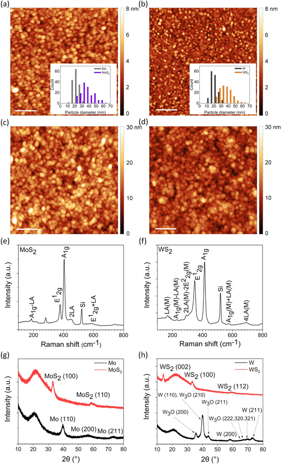
Figure 1. AFM surface topologies of sputter deposited (a) Mo and (b) W thin films as well as their sulfurized derivatives displayed in panels (c) and (d), respectively. Scale bars indicate 200 nm. Insets show the evolution of particle size in the films before and after sulfurization. Raman spectra of sulfurized (e) Mo and (f) W confirming the corresponding phases in the thin films are MoS2 and WS2. Panels (g) and (h) are the respective x-ray diffraction patterns acquired using grazing incidence setup including the original and sulfurized W and Mo films.
Download figure:
Standard image High-resolution imageRaman spectra of the films displayed in figures 1(e) and (f) indicate the materials are crystalline MoS2 and WS2, respectively [25, 26]. Two strong peaks are observed for MoS2 at 378 and 405 cm−1 that correspond to the in-plane (E12g) and out-of-plane (A1g) vibration modes [27]. According to the difference of Raman shifts and also to the intensity ratio of these two peaks, MoS2 is multi-layered [28]. Likewise, the WS2 film has two intensive peaks at 349 and 415 cm−1 that can be assigned to in-plane (E12g) and out-of-plane (A1g) vibration modes, evidencing that the structure is multi-layered [29, 30]. The presence of the longitudinal acoustic mode vibrations (LA) and their higher-order harmonics (2LA and 4LA) are also visible in the spectra. The low intensity of the 2LA peaks confirms the chalcogenides are multi-layered [26]. Note, that in each spectrum, the relatively intensive peak at around 520 cm−1 is due to the Si substrate.
Grazing incidence x-ray diffraction patterns of the original and sulfurized metal films are displayed in figures 1(g) and (h). The metal films pattern fits well the reference patterns PDF 42-1120 and PDF 01-1204 for Mo and W, respectively. In addition, the metallic tungsten film shows some W3O which is indexed according to PDF 02-1138. The pattern of MoS2 shows two strong reflections at 33.2° and 59.5°, which may be indexed as the (100) plane and superposed reflections from the (110) and (008) planes of the hexagonal form of the crystal (PDF 75-1539). However, the strong reflections of the (002) and (102) planes at 14.1° and 36.0° of layered structure that should be also present in the pattern are missing from our diffractogram suggesting the lack of long-range order in stacking of the layers in the material. Another explanation might be a specific crystal orientation on the substrate with basal planes being perpendicular to the surface. However, this latter option is unlikely, since the AFM images show spherical particles on the surfaces that do not resemble oriented crystals. On the other hand, in the case of the WS2 film, the pattern can be assigned to the planes of the hexagonal lattice (PDF 02-0131). The reflection at 14.1° corresponds to the (002) plane, the broad peak at 33.1° is due to the superposed intensities of the (100) and (101), whereas the broad reflection centered at 59.0° can be assigned to the unresolved (110), (008) and (112) planes [29]. It is also worth noting here, that the broad reflection at around 20.0° is due to amorphous SiO2 of the substrate.
The composition of the films was analyzed with EDS (table 1). The aforementioned pinhole defects seen in WS2 films comprise only silicon and oxygen confirming that the defects are indeed voids in the film. Since the thickness of TMD films is ∼20 nm, both Si and O of the Si/SiO2 substrate are visible in the energy-dispersive x-ray spectra even at locations without pinholes. The ratio of sulfur and metal is very close to 2:1 for both TMD films, which implies the films are at least nearly stoichiometric. In the case of WS2 there is a notable amount of C contamination present, which was not observed in MoS2 films.
Table 1. EDS elemental compositions (in at%) averaged for four points of each material.
| C | O | Si | S | W | Mo | M:S ratio | |
|---|---|---|---|---|---|---|---|
| MoS2 | 0 | 44.5 | 48.1 | 5.3 | 0 | 2.1 | 1:2.5 |
| WS2 | 23.5 | 32.4 | 35.9 | 5.4 | 2.7 | 0 | 1:2.0 |
Before the actual sensor measurements, the electrical conductivity of each film was assessed with I–V measurements. Both MoS2 and WS2 films were sufficiently conductive (with resistances of several tens of megaohms and hundreds of megaohms, respectively) to perform sensor measurements on those. The I–V curves were found linear for MoS2, whereas WS2 showed slight nonlinearity (figures 2(a) and (d), respectively), suggesting a barrier between the semiconducting film and the Ti/Pt electrodes [31]. Although the primary direct contact with the chalcogenide films was meant to be Ti, some Pt also deposited on the films around the perimeter of the Ti under-metallization due to the imperfect contact between the shadow mask and the substrate. Considering the typical bandgap, electron affinity and the work function values of bulk MoS2 (Eg ∼ 1.3 eV, χ ∼ 4.0 eV and φ ∼ 5.25 eV)[32, 33] and WS2 (1.4, 4.0 and 5.1 eV) [34] as well as the work function values of Ti (φTi ∼ 4.3 eV) and Pt (φPt ∼ 5.3 eV), we find that the contact between Ti and the chalcogenide films is Schottky-type (figures 2(b) and (e)), whereas it is quasi-ohmic with Pt (figures 2(c) and (f)). Furthermore, because of the better alignment of the Fermi level of Pt with the valence band of MoS2 in reference to WS2, the ohmic character is also expected to be better, which explains the good linearity of the I–V slopes and higher conductivity for the MoS2 based devices and slight nonlinearity measured for the WS2 based ones.
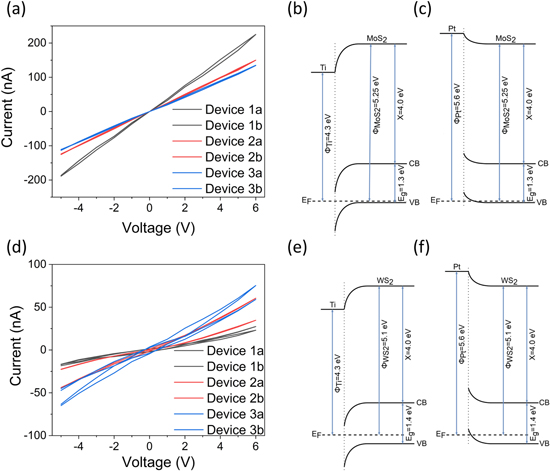
Figure 2. IV curves of (a) MoS2 and (d) WS2. Three sensor devices with two pairs of electrodes, totaling six samples, were measured for each material. The metal–semiconductor junctions for the films and contact electrodes of titanium and platinum are presented in (b), (c) for MoS2 and (e), (f) for WS2, respectively. Note: the energy values used for depicting the band diagrams may not be entirely accurate, as each value shows variation depending on the structure and method of determination, as shown in table S1, available online at stacks.iop.org/NANO/30/405501/mmedia in the supplementary information.
Download figure:
Standard image High-resolution imageIn general, WS2 based devices were electrically less conductive but had considerably higher response to the analytes, although with higher device-to-device variation (average of six devices for each gas) in reference to MoS2 sensors (figures 3 and 4(c)). The films show a small response to H2 (0.00005 ± 0.00003 ppm−1 and 0.00016 ± 0.00017 ppm−1 for MoS2 and WS2, respectively). This is comparable to previous results with WS2 nanowire/nanoflake hybrid structures [18]. For H2S and CO the responses were either nonexistent or inconsistent. Regardless of the variance of the response to other analytes, for NH3 the devices display a consistent and very good response (0.0026 ± 0.0022 ppm−1 and 0.0586 ± 0.0305 ppm−1 for MoS2 and WS2, respectively).
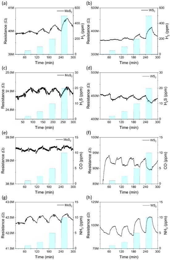
Figure 3. Baseline corrected responses to MoS2 ((a), (c), (e), (g) for H2, H2S, Co and NH3) and WS2 films ((b), (d), (f), (h), respectively). Note: the responses represent the best performing sample of the material for the particular analyte.
Download figure:
Standard image High-resolution image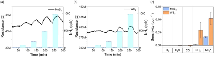
Figure 4. Response of MoS2 (a) and WS2 (b) for sub-ppm levels of NH3. (c) Average sensitivities for each gas calculated for the smallest observable responses measured in the ppm range. Data for NH3* shows the sensitivity measured at 200 ppb for both MoS2 and WS2.
Download figure:
Standard image High-resolution imageSince the response to NH3 with both sensors was very distinct at 1 ppm gas concentration, additional measurements were performed in the sub-ppm NH3 concentrations. Significant responses to 200 ppb of the analyte could be measured with average sensitivities of 0.0315 ± 0.00282 ppm−1 and 0.104 ± 0.0243 ppm−1, respectively (figure 4). According to the signal to the base noise ratio, the limit of detection (LOD) is under 100 ppb for both materials. The response time of the MoS2 based sensors to the analytes were found to be rather short for NH3 (5–6 min) and slightly longer for other gases (10–30 min). The sensor recovery time constants were long (30–60 min) and varied greatly among the gases. On the other hand, sensors made of the WS2 films showed a consistent and quick (5–6 min) response and recovery for each gas, which is excellent considering that the measurements were carried out at near room temperature.
According to the reducing nature of all the analyte gases and the response of the sensors, it can be concluded that both WS2 and MoS2 exhibit p-type semiconducting behavior, and the resistance of the sensors increase with the concentration of the analytes. This is usually explained by surface adsorption and subsequent charge transfer based mechanisms; the reducing gases donate electrons (or localize holes) in the materials, thus reducing the concentration of charge carriers, and consequently reduce the conductivity of the material [18, 20]. A number of other studies show selectivity to NH3 for both WS2 [22, 23, 31, 35] and MoS2 [20, 36, 37]. In the case of MoS2, the LOD of 100 ppb is similar to other results (300 ppb measured and 50 ppb predicted) [24]. In the case of WS2, the reported LODs are about a decade worse (∼1 ppm)[38, 23] than our data. (In table S2, we list a more detailed comparison of the results with other reported values for MoS2 and WS2 based devices and commercial NH3 sensors.)
As the sensing behavior of the thin films presented in the manuscript is similar to or better than those reported for other MX2 based devices regarding NH3, we may assume that the sensing mechanism is also similar, i.e. associated with surface adsorption and consequent partial charge transfer. Calculated (local-density approximation, LDA) surface adsorption energies of H2, NH3 and CO on MoS2 with corresponding values of −82 meV, −250 meV and −128 meV, respectively, also seem to support the high response to NH3 on MoS2 films [20, 39]. Similarly, on WS2, the calculated energies [18] are –57.4 meV (H2), –171.7 meV (NH3). and −84.7 meV (CO) indicating that the response to NH3 is expected to be the highest. Here, we have to point out another effect regarding H2S. Namely, considering the high adsorption energy of H2S (−181 meV) on WS2 nanosheets, we shall also expect to see good response to H2S. However, this is not the case with our thin films. The reason is that competitive lattice doping with O and S is responsible for the detection of H2S as we have concluded in our earlier work [18] based on XPS analysis of WS2 nanowire-nanoflake hybrid structures, in which nanosheets of ∼5 nm thickness were sticking out from the surface of the nanowires. The structure is different now, since both WS2 and MoS2 films are comprising nanoparticles of 20–30 nm in their diameter with limited diffusion of O and S in the lattices, thus despite the large adsorption energy of H2S, the sensor response is insignificant to this analyte.
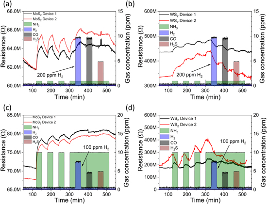
To analyze the cross-sensitivity of the sensors, we performed two sets of measurements for two samples of each material (figure 5). In the first set, we applied gas pulses with concentrations of 1 ppm, 200 ppm, 10 ppm and 5 ppm for NH3, H2, CO and H2S, respectively. In the other set, the respective concentrations were 10, 100, 5 and 5 ppm. The sensitivity to NH3 remained high for all samples throughout the measurements (the first three pulses in each plot), which proves the repeatability and reproducibility of the devices. During the long 4th pulse of NH3 (starting at 300 min) we introduced also H2, then CO and H2S for short intervals (30 min each starting at 330 min, 390 min and 460 min, respectively) to see the influence of the secondary analytes. The MoS2 film was affected only by H2 but only when its concentration was high relative to the concentration of NH3 (figure 5(a)). The influence of secondary analytes on the response to NH3 introduced at similar concentrations was insignificant (figure 5(c)). However, in the case of the WS2 based device, we observe a decreased response to low concentration NH3, when introducing the other gases at high concentrations (figure 5(b)). The effect is lower, when the analyte concentrations were adjusted to be similar (figure 5(d)). The results measured with WS2 sensors indicate, that the secondary gas pulses clan flush away the surface adsorbed NH3 thus influencing the sensor performance.
Figure 5. Cross-sensitivity analysis of the sensors using (a), (b) low concentration NH3, and high concentration H2, CO and H2S pulses as well as (c), (d) similar analyte concentrations during the measurements.
Download figure:
Standard image High-resolution image
Furthermore, it is worth pointing out that all sensors were operating in a rather reliable and repeatable manner throughout a period of more than nine month testing in various experimental conditions, which indicates that the thin film WS2 and MoS2 structures are very robust and practical.
Conclusions
A method to produce MoS2 and WS2 thin films by simply annealing sputtered Mo and W films in S vapor is proposed, and the gas response of the as-synthesized films are examined in the classical resistive sensor arrangement. Both materials showed excellent selectivity for NH3 with very high corresponding sensitivity values (0.03 ± 0.0 ppm−1 and 0.10 ± 0.02 ppm−1, respectively) at 30 °C. Despite the low operation temperature, the WS2 based sensors responded to the stimuli and then recovered after each gas pulse quite fast (5–6 min). The results obtained with our robust TMD films compete with other exfoliated or CVD grown single or few-layer chalcogenides and outperforms metal oxides. Since the process steps involved apply standard techniques, up and down-scalable, and the films produced are easy to process further (e.g. coating with other materials) the results presented in this paper may pave the road for sensor applications of TMD thin films.
Acknowledgments
Support received from the Väisälä Foundation, Riitta and Jorma J. Takanen Foundation, Academy of Finland (298409), University of Oulu (Project: Entity) and European Union Interreg Nord – Lapin liitto (Project: Transparent, conducting and flexible films for electrodes) are acknowledged. Kai Metsäkoivu (Center of Microscopy and Nanotechnology, University of Oulu) is acknowledged for the metal films deposition.
Conflicts of interest
The authors declare no conflicts interest.