

Abstract
We report on the direct observation and simultaneous use of the linear and quadratic electro-optical effect and propose a method by which higher-order susceptibilities of electro-optical materials can be determined. The evaluation is based on the separation of the second- and third-order susceptibilities and the experimental technique uses a slot waveguide ring resonator fabricated in integrated photonic circuit technology, which is embedded by a guest-host polymer system consisting of the azobenzene dye Disperse Red 1 in a poly(methyl methacrylate) matrix as an active electro-optical material. The contribution of both effects on the electro-optical response under the influence of static and time-varying electrical fields is investigated. We show that the quadratic electro-optical effect has a significant influence on the overall electro-optical response even with acentric molecular orientated molecules. Our findings have important implications for developing electro-optical devices based on polymer-filled slot waveguides and give rise to advanced photonic circuits.
Export citation and abstract BibTeX RIS

Original content from this work may be used under the terms of the Creative Commons Attribution 3.0 licence. Any further distribution of this work must maintain attribution to the author(s) and the title of the work, journal citation and DOI.
1. Introduction
Silicon-organic hybrid (SOH) photonics have received massive research interest because they combine the advantages of well-established silicon-on-insulator (SOI) technology with that of highly efficient electro-optical (EO) polymers [1]. In recent years, slot waveguides have pushed the hybrid integration of EO polymers in mature SOI technology, since they allow a large overlap of the optical and electrical field inside the polymer-cladding. Such EO polymers typically rely on either the linear EO effect [2] or on the quadratic EO effect [3].
SOH-based modulators have shown a lower signal chirp and therefore better signal linearity compared to modulators employing the plasma dispersion effect [4]. Moreover, SOH modulators are extremely energy-efficient in terms of energy per-bit consumption [5] and can overcome limitations of current modulators based on the plasma dispersion effect with regards to speed, noise and power consumption [6]. This relies on the high values of the electric fields attainable with small electrode separation, able to induce a more effective refractive index change with respect to rejection/removal of charges. In fact, the electric field induces a delocalization of electrons along the conjugated polymer chain and, thus, no carrier transport is necessary, as is required in case of the plasma dispersion effect. The ability to use organic materials in a silicon-on-insulator (SOI)-technology has created significant interest in various fields of science, including but not limited to high-speed modulators [7], tunable optical filters [8], high-precision metrology [9] and frequency combs [10].
However, the hybrid integration of nonlinear optical materials in a SOI technology platform is still a focus of current research. Both effects, the linear and the quadratic EO effect, are the main subjects in this progress and need to be carefully analyzed. The research to date has tended to focus on the linear EO effect rather than quadratic EO effect [11, 12]. However, both effects are present simultaneously in acentric materials and current research has demonstrated that the quadratic EO effect in slot waveguide structures becomes significantly strong [3, 13, 14]. Therefore, current studies may tend to overestimate the linear EO effect because they neglect the quadratic EO contribution. Both EO effects receive great interest for programmable and reconfigurable photonic circuits since they provide different EO responses and, hence, different device concepts can be envisioned. Therefore, the precise analysis of both EO contributiions is crucial for the device design.
During the last few decades, several works were published addressing the simultaneous determination of the linear and quadratic EO effect in bulk material, e.g. using the modified Teng–Man technique [15]. These efforts provided a better knowledge of both effects and supported the development of new organic EO materials. In practice, however, it is difficult to obtain reliable information from this type of measurement, as the quadratic EO response is close to the detection limit. Moreover, since high-voltages are necessary to induce an adequate electric field to obtain the quadratic EO effect, voids and air gaps can easily lead to a breakdown and therefore the samples are usually baked at glass transition temperature under mechanical pressure [16], which makes the sample preparation relatively extensive.
This paper is devoted to describe an experimental on-chip measurement technique to determine both effects simultaneously, while sophisticated sample preparation and high poling voltages are avoided. An experimental approach is presented by which higher-order susceptibilities of EO materials can be determined. The evaluation is based on the separation of the second- and third-order susceptibilities and the experimental technique uses a SOH slot waveguide phase shifter implemented in a silicon ring resonator. The scope of the present paper is to set the experimental conditions under which the present technique constitutes a good investigation tool. In addition, the application of both effects for intensity modulation is presented and the conditions to achieve them separately are described.
2. Theory
Linear and quadratic EO effects are simultaneously present in materials with acentric molecular order. In isotropic materials, the linear EO effect vanishes and only the quadratic EO effect is observable. A poling procedure is required to obtain an acentric molecular order from an isotropic material. There are different poling procedures such as optical poling [17], corona poling [18] and contact poling [19]. However, since the slot waveguide requires an optical transverse electric (TE) field mode to avoid optical losses [20], the nonlinear optical molecules need to be aligned parallel to it in order to achieve a large linear EO effect [21]. Therefore, it is reasonable to employ contact poling, in which the slot waveguide forms the electrodes allowing for a strong electric field parallel to the electric field component of the optical TE-mode [14]. A comprehensive analysis of the poling procedure and implications of the narrow gap of the slot waveguide on the poling efficiency can be found in [11]. However, the EO material is in between the electrodes and exhibits an intrinsic polarization. As a consequence, the molecules are orientated along the electric field breaking the centrosymmetry of the isotropic EO material. To obtain a measurable effect, the EO material is heated up near to its glass transition temperature. However, this state is not stable due to thermal effects and, therefore, the material is cooled down to ambient temperature while the electric field is still applied. This yields a temporal acentric molecular order.
The EO effect is usually considered in terms of the change of the optical indicatrix [22]
where rijk and Rijkl are the Pockels coefficient and Kerr coefficient, which describe the linear and quadratic EO effect, respectively. For small changes and anisotropic materials, the refractive index change  along the main direction of the optical indicatrix can be approximated by [23]
which can also be expressed by using the nonlinear optical susceptibility tensor
Comparing the coefficients in equations (2) and (3) yields the relations
For an EO material in a vertical slot waveguide, the dominant tensor components are represented by  and
and  . In this case, the optical and electrical field are orientated along the 3rd axis. Therefore, this case will be considered throughout this work and the notation
  and
and  will be used, for the sake of simplicity. Additionally, we assume an approximately isotropic refractive index of the EO polymer at the absence of an electric field, which will be referred to as neop.
One key statement of the present work is that the quadratic EO component  of linear conjugated polymers in slot waveguides is not negligible. As a consequence, it has to be taken into account for the calculation of the linear EO component
  since the quadratic EO effect is obtained in any molecular order. The proportion
gives an estimation of the contribution of the quadratic EO effect on the overall refractive index change. Here, the overall refractive index change is given by the the sum of the linear EO effect (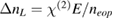 ) and quadratic EO effect (
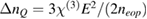 ) in the denominator. As an example, we have determined
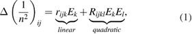
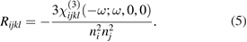
  using values from [24] and plotted the results in figure 1. It is apparent from this figure that the quadratic EO effect is negligible in bulk material but may contribute
  to the overall refractive index change in slot waveguides. Therefore, a technique to separate the quadratic EO effect from the linear EO effect directly from the measured on-chip performance is beneficial. In the following, a method to infer
  and
and  from a static EO response is provided.

Figure 1. Calculated refractive index change induced by the linear and quadratic EO effect as a function of the slot width. The quadratic EO effect is inversely proportional to the square of the electrode distance, which is in fact the slot width s. Parameters:  , neop = 1.71,
 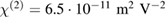 ,
,  .
.
Download figure:
Standard image High-resolution image3. Device fabrication and sample preparation
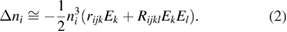
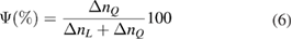
To validate our theoretical assumption, we employ a silicon ring resonator covered with an EO polymer. Here, a partially slotted ring resonator (PSRR) is used consisting of a slot waveguide phase shifter introduced in the straight part of a racetrack ring. A schematic of the PSRR is shown in figure 2(a). The slot waveguide is connected through doped silicon striploads and tungsten vias to ground-signal-ground (GSG) metal electrodes, as shown in figure 2(b). Vertical silicon slot waveguides have the advantage of a strong overlap of optical and electrical field [25]. Details on the ring resonator geometry and fabrication details can be found in our previous work [8, 26–28]. In this work, we employ a PSRR having a slot waveguide length of  and a slot width of
  .
.

Figure 2. (a) Schematic representation of the partially slotted ring resonator. The slot waveguide phase shifter is introduced in the straight part of the racetrack ring resonator. (b) Cross-sectional view of the slot waveguide phase shifter. (c) Structural formula of DR1 and PMMA. (d) Dispersion curves of PMMA/DR1.
Download figure:
Standard image High-resolution imageThe PSRR is fabricated on a  SOI wafer in a photonic integrated circuit (PIC) technology at IHP [29]. Here, we have chosen a slot width of
  to be compatible with the PIC technology. After a cleaning procedure with acetone and 2-propanol, the EO polymer is directly spun onto each chip at
  . We employed the azobenzene dye Disperse Red 1 (DR1) from Sigma Aldrich doped at
  in poly(methyl methacrylate) (PMMA) [30]. The chemical structures are shown in figure 2(c). This guest-host polymer system is solved in 1.1.2.2-tetrachloethane and filtered through a PTFE-membrane filter with
  pores. To remove the solvent after deposition on the chip, we have dried the samples at
  in an oven.
In addition, we have prepared bulk polymer films in order to obtain material properties of PMMA/DR1. Spectroscopic ellipsometry (Sentech SE 850) was carried out to measure the refractive index, which was supported by spectroscopic photometry data (PerkinElmer Lambda 1050). The dispersion is plotted in figure 2(d). Here, the DR1/PMMA thin film was modelled with the Bruggemann effective medium approximation. A Sellmeier model was employed for the non-absorbing PMMA matrix and the Tauc-Lorentz oscillator model for DR1. From figure 2(d), it can be inferred that within the studied wavelength range (optical C-band), the EO effects are off-resonant since it is far away from the first resonance peak.
4. Experiments
4.1. Measurement of higher-order susceptibilities using a slot waveguide ring resonator
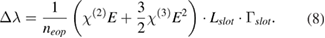
The refractive index change  of the polymer correlates directly to a phase shift in the slot waveguide given by
  [3], where Lslot is the slot waveguide length,
  is the wavenumber and
  is the field confinement factor in the slot region. The latter is taken into account to avoid an overestimation of the phase shift
  [31]. In principle, it can be defined as the ratio of the time averaged energy flow through the slot region to the time averaged energy flow through the total domain [32]. It can be calculated by [33]
Here, E and H are the electric and magnetic field vectors, respectively, and ez is the unit vector in the z direction. The slot region and the total domain are denoted as slot and total, respectively. The field confinement factor for the given waveguide geometry is  according to our simulation study [31, 34]. A more comprehensive description of the aforementioned measurement technique can be found in [3, 14].
Applying a DC voltage U to the slot waveguide leads to an electric field inside the slot by E = U/s. This assumption is valid since the electric field is approximately homogeneous inside the slot. Taking the relation  into account, the applied voltage leads to a resonance wavelength shift given by
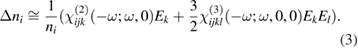
We obtained the wavelength shift  from the transmission spectra at different DC voltages. The experimental set-up is schematically shown in figure 3. Here, a tunable external cavity laser (Yenista TUNICS T100S-HP) is used in order to measure the wavelength dependent behavior of the ring resonator. The polarization of the laser light was adjusted in such a way that highest transmission is achieved by using a paddle style fiber polarization rotator (Thorlabs FPC031). The light is transmitted through a polarization maintaining single mode fiber and then coupled into the silicon waveguides through a fiber grating coupler. The transmitted light is then coupled by a second grating coupler to a polarization maintaining single mode fiber and then to a photodiode (Thorlabs DET08CFC/M). All measurements were carried out using a temperature-controlled sample holder which was stabilized to
  in order to avoid changes in the transmission due to temperature fluctuation. For active measurements, the GSG electrodes are connected to an electric power source (Keysight Sourcemeter 2400) through tungsten DC probes (Picoprobes A 40A-GSG-150-P). Depending on the experiment, the optical signal is measured with a digital sampling oscilloscope or a digital multimeter.

Figure 3. Experimental set-up: the polarization of an external cavity laser is controlled by a paddle style fiber rotator and coupled to the photonic chip by means of fiber grating coupling. A photodiode translates the optical signal to an electrical. For static electric field measurements, a digital multimeter is used, while for dynamic measurements an digital sampling scope is employed. The electric field inside the slot waveguide is induced by applying a DC or AC signal to the metal electrodes using either a function generator or a DC source.
Download figure:
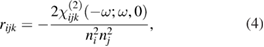
Standard image High-resolution imageWe have performed two experiments. The first is carried out without the poling procedure to determine the quadratic EO effect. In the second experiment, we poled the EO polymer to obtain a non-centrosymmetric molecular orientation of the nonlinear optical dye, which leads to an increase of the linear EO effect. The poling procedure is shown in figure 4. First, the sample is heated up from ambient temperature Ta (figure 4(a)) to the glass transition temperature  for
for  (figure 4(b)). This is followed by applying a poling voltage of
  to align the dye molecules (figure 4(c)), and then the temperature was rapidly reduced to ambient temperature Ta, while the poling voltage was kept on (figure 4(d)). One major issue of organic EO materials is that they suffer from long-term stability due to relaxation processes (figures 4(e) and (f)) [35]. However, with the present technique, we are able to perform the measurement directly after the poling procedure using the same set-up.

Figure 4. Poling procedure: (a) sample at ambient temperature Ta. (b) Sample at glass transition temperature Tg. (c) Applying of poling voltage at glass transition temperature Tg. (d) Cooling down to ambient temperature Ta while poling voltage is kept applied. (e) Sample at ambient temperature Ta without poling voltage. (f) Relaxation process at ambient temperature Ta.
Download figure:
Standard image High-resolution imageIn both experiments, we measured the resonance wavelength shift as function of the applied voltage. The results are plotted in figure 5(a). The experimental data in figure 5(a) is then fitted using a polynomial regression model given by 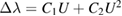 . Please note, the coefficient of determination is >R2 = 0.997 and the residual sum of squares is
  for both graphs, reflecting the high accuracy of the least square fit. A static electric field E = UDC/s was taken into account and equation (8) was compared with our regression model to yield the second- and third-order susceptibility coefficients, which are given by
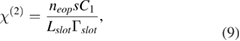
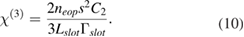

Figure 5. Resonance wavelength shift before and after applying a poling procedure.
Download figure:
Standard image High-resolution imageFrom the data in figure 5, we inferred a second- order susceptibility of 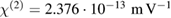 and
and  without poling procedure. After the molecular alignment of the EO dyes through a poling procedure, we observed an increased second-order susceptibility of
  , while the third-order susceptibility keeps approximately the same
  , as shown in figure 5(b). Table 1 summarizes all EO values. Due to the non-optimized poling procedure, the poling efficiency is about 35% compared to the EO coefficient reported in bulk EO polymer films [35]. Polar chromophores like DR1 tend to interfacial interactions with the electrodes and thus do not contribute to poling induced EO activity [11]. Surface/material interfacial effects are magnified in nanoscale slot waveguides, which is also suggested by recent simulation studies [36, 37]. In addition, the time window to conduct the experiment is of importance, since a decay of the linear EO effect is possible due to relaxation processes [35]. In our experiment, we have performed the experiments to observe the linear EO effect right after the poling procedure by simply switching between a high-voltage necessary for the poling procedure to a low-voltage for the conducted experiments with a static as well as time varying electric field.
Table 1. EO response due to different conditions.
Before poling: isotropic  |
After poling: acentric order  |
|
|---|---|---|
 |
 |
 |
 |
0.094 | 2.444 |
 |
 |
 |
 |
 |
 |
However, our findings clearly demonstrate the strong impact of the quadratic EO effect on the overall EO response. In particular, according to equation (1) we have evaluated a contribution of the quadratic EO effect to the overall refractive index change of about  after the poling procedure was applied. This finding suggests that the quadratic EO effect is not negligible in narrow slot widths.
4.2. Intensity modulation using the linear and quadratic EO effect
In this section, we show the influence of both EO effects on intensity modulation. Inserting the electric field 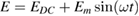 into equation (2) yields an expression for the time-varying refractive index change

comprising a static refractive index change  , a time-varying refractive index change
  due to the quadratic EO effect and a time-varying refractive index change
  due to the linear and quadratic EO effect, where
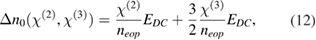
Since the static electric field EDC is fixed, equation (12) is a constant and has no influence on the modulated optical signal. In fact, this term induces an offset of the resonance peak and has to be taken into account to find the operation point, which typically lies in the linear regime of the resonance peak. Equation (13) is solely influenced by the quadratic EO effect and gives a sine-squared signal. Figure 6(a) shows a schematic overview of all possible scenarios and experimentally obtained EO responses (oscilloscope traces) for each case. In contrast, equation (14) shows that the sine response is affected by the linear and the quadratic EO effect. Note that the term  in equation (14) is also known as the electric field-induced second-order nonlinear optical effect [38]. To distinguish between the
  and
and  contribution we define two cases. In the first case, the EO response is characterized by a sine-squared signal if
  , as shown in figure 6(a). In the second case, the EO response shows a sine signal if
  (figure 6(b)). In this way, it is possible to observe a linear response by applying an offset voltage
  in an isotropic material (centric order).
Figure 6. Schematic representation and experimentally observed oscilloscope traces of the EO response: (a) the electric modulation field (blue) induces a sine squared modulated optical field (green) if  and
and  . (b) If the symmetry is broken and
  , the electric modulation field (blue) is causing a sine modulated optical field (green) and a small refractive index offset due to the nonlinear response curve. (c) If an offset voltage is applied and the modulation amplitude is small enough (
 ), the modulated optical response follows a sine function. (d) Applying an offset voltage to a acentric material leads to a larger refractive index offset but also to a larger EO response due to the nonlinear response curve.
Download figure:
Standard image High-resolution image
However, an acentric molecular order can be obtained by applying a poling procedure. In this case, the observed EO response is characterized by a sine signal as well (figure 6(c)), since the second-order effect dominates the third-order one. Applying an offset voltage gives approximately the same signal, as shown in figure 6(d).
An implication of our findings is that both linear and quadratic EO effect should be taken into account when extracting material properties from experimentally observed phase shifts. In the present work, we have determined the higher-order susceptibility tensor components  and
and  . In the case where one wishes to use the material for devices based on second harmonic generation and on the optical Kerr effect, it is necessary to correct our results by the dispersion in order to retrieve the evaluation of the
 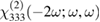 and
and  tensor components [15].
5. Conclusions
We have presented a method by which higher-order nonlinear optical susceptibilities of EO polymers can be determined. A silicon slot waveguide ring resonator fabricated in a photonic integrated circuit technology was used to observe the EO response and we applied our model to the nonlinear optical dye DR1 doped in PMMA. We have analysed the EO response before and after applying a poling procedure. It is revealed that the quadratic EO effect has a significant impact on the overall EO response even with an acentric molecular order due to the strong electric field inside the slot waveguide. As a consequence, our findings implicate that both the linear and quadratic EO effect should be taken into account when extracting material properties from experimentally observed phase shifts in nano-scale slot waveguides. With the presented method, it is possible to distinguish between the linear and the quadratic EO response, which is an important step for the design and validation of future reconfigurable and field-programmable photonic devices based on slot waveguides and for the evaluation of EO material properties.
Acknowledgment
This work is funded by the European Regional Development Fund (10.13039/501100008530).