

Abstract
To replace mercury lamps with AlGaN-based deep-ultraviolet (DUV) LEDs, a simple and low-cost package with increased light extraction efficiency (LEE) is indispensable. Therefore, resin encapsulation is considered to be a key technology. However, the photochemical reactions induced by DUV light cause serious problems, and conventional resins cannot be used. In the former part of this study, a comparison of a silicone resin and fluorine polymers was carried out in terms of their suitability for encapsulation, and we concluded that only one of the fluorine polymers can be used for encapsulation. In the latter part, the endurance of encapsulation using the selected fluorine polymer was investigated, and we confirmed that the selected fluorine polymer can guarantee a lifetime of over 6,000 h at a wavelength of 265 nm. Furthermore, a 3 × 4 array module of encapsulated dies on a simple AlN submount was fabricated, demonstrating the possibility of W/cm2-class lighting.
Export citation and abstract BibTeX RIS
1. Introduction
AlGaN-based deep-ultraviolet (DUV) (λ < 300 nm) LEDs are expected to be useful for sterilization, deodorizing, ultraviolet curing, and so forth. AlGaN-based DUV LED bare dies have achieved an external quantum efficiency (EQE) greater than 5%1) at 280 nm without any light extraction enhancement by using, for example, photonic crystals,2,3) and encapsulation,4–6) transparent p-cladding layer and reflective electrodes.7,8) Also, we demonstrated an EQE of more than 3%2) between 255 and 300 nm, and we have recently obtained EQEs of more than 6.1, 3.9, and 3.5% at 283, 271, and 266 nm, respectively.9) Note that our EQE results in Refs. 1, 2, and 9, were obtained without any light extraction enhancement and measured through a calibration with the standard light source (L-7810-02) fabricated by Hamamatsu. When a thick p-GaN contact layer was incorporated, the light extraction efficiency (LEE) of bare dies is considered to be limited to about 8%.10) Accordingly, our AlGaN-based DUV LEDs on sapphire substrates within a wavelength range from approximately 265 to 300 nm are considered to have high IQEs (as high as 80%), presumably owing to the carrier localization due to ternary disordering9,11) and AlGaN templates with low threading dislocation density.12) This means that there is little room for improving the IQE of DUV LED dies. From the above background, increasing the LEE should be a priority to enable the practical use of DUV LEDs. As a means of increasing the LEE, we consider that encapsulation is highly desirable when we pursue low resistivity p-contact and low-turn-on-voltage incorporation of thick p-GaN contact layers. Since the photon energy of DUV light is as high as 4.1 eV at 300 nm, most organic compounds will be destroyed by the molecular dissociation induced by DUV light. Among the resins with robustness against ultraviolet light, Si–O- and C–F-based polymers are considered to be candidate encapsulation materials. In our recent works on C–F-based polymers, we compared the main-chain of different amorphous fluorine polymers13) and concluded that polymerized perfluoro-4-vinyloxy-1-butene (BVE), having a 5-membered ring with a single oxygen,14) is suitable from the industrial viewpoint. By comparing BVE-based polymers having terminal molecules of trifluoromethyl (–CF3) and carboxylic acid (–COOH), we concluded that –COOH damages the electrode and causes short circuits.4) To solve this problem for the –COOH group, the coauthors proposed the use of a BVE-based polymer terminated with methoxy (–COOCH3) end groups, expecting less damage to the electrodes because of the lack of an –OH structure, which is one of the most reactive structures. Therefore, in addition to the end groups of –CF3 and –COOH, we conducted a feasibility study on a BVE-based polymer terminated with –COOCH3. Furthermore, a detailed investigation of Si–O-based polymers from the viewpoint of encapsulation for DUV LEDs is reported. In this work, we compared polymers having potential for the durable encapsulation of DUV LEDs.
In the former part of this work, we describe the degradation mechanism of a state-of-the-art silicone resin15) with reasonably high transparency at a wavelength of 250 nm, which is considered to be the most robust against DUV light among the silicone polymers. For the silicone resin, the cracking induced by DUV irradiation caused a decrease in LEE. On the other hand, a BVE-based polymer termination with –COOCH3 caused serious leakage due to the photochemical decomposition induced by DUV light, similar to the case of termination with –COOH.4) Following detailed evaluations of the above polymers, endurance tests focusing on the degradation of bulk resin were carried out using a BVE-based polymer terminated with –CF3, and no significant damage was observed in the encapsulation layers within 10,000 h.
In the latter part, we demonstrate a chip-on-board (COB) package using the fluorine resin selected through the feasibility study in the former part. To replace conventional mercury lamps, it is a problem for DUV-LEDs to be competitive. However, the package also needs to be robust against DUV light, meaning that a ceramic mount is indispensable. In addition, it is desirable to inject a higher density current to the mesa cross section to obtain a higher output. Although a thick p-GaN contact layer is applied, the driving DUV LEDs at approximately high voltage of 5–7 V1,2,9) require high heat dissipation compared with conventional LEDs. Thus, a COB package on an AlN ceramic sheet is thought to be suitable for practical applications. With the goal of realizing packaged DUV LEDs, single hemispherical encapsulation layers on an AlN submount were fabricated using a molding technique and the LEE was increased by a factor of ×1.5. Moreover, a 3 × 4 array module was fabricated using a mold with 12 hemispherical concave depressions, keeping the mass production of COBs on an AlN ceramic sheet in mind. The LEE of the array module increased by a factor of ×1.5 and the array module recorded an output of 472 mW at 280 nm at a driving voltage and a current of 63 V and 200 mA, respectively.
2. Molecular structures and characteristics of DUV-transparent polymers
Candidate resin encapsulation materials are limited to Si–O- and C–F-based polymers, whose molecular structures are shown in Fig. 1. The selection of the C–F main-chain structure was discussed in our work13) and the only C–F polymer used in this work was a C–F polymer with a basic structure of polymerized BVE having a 5-membered ring with a single oxygen atom. As a Si–O-based resin, we selected a silicone resin considered to be among the most robust against DUV light.15) Figure 1(a) shows the basic structure of a one-dimensional silicone resin having silica particles that act as a junction between one-dimensional silicone polymers. Here, "R" can be changed in accordance with the desired properties of the silicone resin. For example, the robustness against DUV light will be lost upon the incorporation of a benzene-like molecule to obtain a higher refractive index. Therefore, we chose a silicone with R=CH3, which was expected to maximize the robustness against DUV light. Figure 2 shows the transmittance spectra of all the polymers having a significant window in the DUV region, which are compared in our feasibility study. The silicone resin has a transmittance window at wavelengths longer than 250 nm, although a weak absorption was observed at wavelengths shorter than approximately 300 nm. The absorption edge at 250 nm was considered to originate from Si–O, and the weak absorption at wavelengths shorter than 300 nm might have originated from the polymerization initiator, which must be used with silicone polymers. Note that polymerization initiators are difficult to remove because they are dispersed in the precursors of silicone resins. For the BVE-based fluorine polymers, there are several choices of the end molecule in terms of observing the transmittance window. We previously reported a detailed comparison of –COOH with –CF3.4) However, we have not compared –CF3 with –COOCH3, which has a promising window and results in less damage to the electrode than that in the case of –COOH.

Fig. 1. Molecular structures of (a) silicone with simple –CH3 side chains and (b) amorphous fluorine polymers obtained by polymerization of BVE, with various terminal ends indicated by –R.
Download figure:
Standard image High-resolution image
Fig. 2. Transmittance spectra of a silicone resin and three types of fluorine polymer used in this paper. Thicknesses of silicone and fluorine samples were 1.0 mm and 200 µm, respectively.
Download figure:
Standard image High-resolution image3. Comparison of silicone and fluorine resins
3.1. Degradation of silicone encapsulation layers and its mechanism
An encapsulated sample of the AlGaN-based DUV LED was prepared on an AlN submount (5 × 5 mm2) attached to aluminum reflectors. The bare dies were mounted using Au bumps, then underfilled and encapsulated using the same silicone. The underfilling and encapsulation involved the use of the potting method with a dispenser, which was followed by thermal setting at 150 °C. Figure 3 shows photographs of typical samples after the endurance tests, and Fig. 3(a) shows a photograph of an entire sample with the inset showing the damage. The die size used in these tests was 1.3 × 1.3 mm2 with a mesa cross section of 0.66 mm2. After the endurance tests, the cracks above the dies were observed for the samples exposed to 270, 285, and 300 nm DUV light, as respectively shown in Figs. 3(a)–3(c). In the cases of 270 and 285 nm DUV light, cracks were first observed after 397 and 1025 h at a current of 250 mA, respectively. For the 300 nm sample, the current was set to 400 mA to accelerate the test, and cracks were first observed after 1050 h. To separate the effects of encapsulation and the LED die, the light extraction enhancement ratio (RLEE) is plotted in Fig. 4 for multiple samples with and without encapsulation. For the samples exposed to 300 nm DUV light, the average initial output of bare chips before the encapsulation was almost the same ( ) as that of the bare chips that were prepared for the samples without encapsulation. RLEE was simply calculated as the output with encapsulation divided by that without encapsulation. For the samples exposed to 285 nm light, the average initial outputs of bare chips were different between encapsulated and nonencapsulated groups. The open and solid circles in Fig. 4(b) indicate the results for the samples with and without the compensation of the difference in average initial output, respectively. Note that RLEE decreased when a crack occurred in both cases, despite stable bare die outputs. Thus, the decrease in output was determined to be caused by the cracks in the encapsulation layers. The degradation mechanism of silicone by short-wavelength UV light is commonly understood. However, the justification of our selection of silicone is necessary. Thus, measurements of the changes in hardness and the weight loss due to the irradiation of 254 nm DUV light were carried out using bulk silicone. The bulk sample had a hardness of 6 HDA without DUV irradiation. Note that HDA is a widely used unit to indicate the hardness of a rubberlike material. After irradiation for 6 and 12 h, the hardness changed to 13 and 20 HDA, respectively. This is considered to be due to the additional polymerization, which is thought to form cross-links between one-dimensional silicone polymers. The weight of the bulk sample was reduced to 99.85 and 99.67% of the nonirradiated sample after the irradiation for 6 and 12 h, respectively. This weight loss also supports the hypothesis of the additional UV-induced polymerization. To determine the effect of the –CH3, further investigation by Fourier-transform infrared (FT-IR) spectroscopy was carried out. Figure 5 shows FT-IR spectra of the silicone resin exposed to 254 nm irradiation for 0, 12, and 24 h. H2O-related peaks developed between 2500 and 3500 cm−1 after the irradiation, indicating dehydrocondensation, showing the occurrence of the additional polymerization. Also, the CO-related peaks between 1700 and 1750 cm−1 became stronger after the irradiation, implying the effect of –CH3 side chains, consistent with the formation of cross-links between one-dimensional silicone polymers. These results agree with the conventional decomposition mechanism of the silicone resin. Accordingly, despite the robustness of Si–O bonds against DUV light, Si–C bonds were considered to be destroyed by DUV light. Consequently, although the silicone polymer was carefully selected, the silicone resin is considered to be unsuitable for the encapsulation of DUV LEDs.
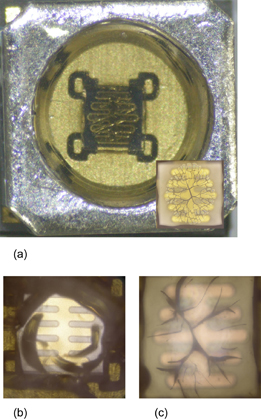
Fig. 3. Photographs of the cracks occurring above the DUV LED dies after the endurance tests with DUV light of (a) 270, (b) 285, and (c) 300 nm. In (a), a photograph of the entire encapsulated sample is shown and the inset shows the cracks above the die.
Download figure:
Standard image High-resolution image
Download figure:
Standard image High-resolution image
Fig. 4. Endurance results of the samples with and without encapsulation exposed to DUV light of (a) 300 and (b) 285 nm in the case of silicone resin. The light extraction enhancement ratio (RLEE) is estimated by dividing the output of the encapsulated sample by that of the sample without encapsulation. Note that, for (b) 285 nm, the open circles indicate the data calibrated using the average initial output power.
Download figure:
Standard image High-resolution image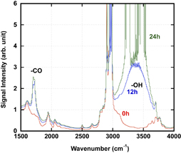
Fig. 5. FT-IR spectra of silicone resin as thermally set and after 12 and 24 h exposure to 254 nm DUV irradiation. –CO- and –OH-related spectra appeared after the DUV irradiation, showing additional polymerization induced by DUV light.
Download figure:
Standard image High-resolution image3.2. Endurance tests of fluorine resins and comparison of silicone resin with three BVE-based polymers
In addition to the BVE-based fluorine polymers terminated with –CF3 and –COOH, we evaluated the electrode degradation for another BVE-based resin terminated with –COOCH3. Following our previous report,4) a sample terminated with –COOCH3 was proposed by Asahi Glass. The –OH in the –COOH ends was considered to cause serious electrode degradation, and we thus expected less degradation upon using –COOCH3 ends. A bare chip without underfilling and overcoating was prepared as a reference. Figure 6 shows the microscopy images of the electrodes after the endurance test for the cases of fluorine polymers with –CF3, –COOH, and –COOCH3 ends and the bare chip, which are denoted as S, A, E, and N/A, respectively. The size of each die was 800 × 800 µm2 with a mesa cross section of 0.16 mm2. Compared with the –COOH ends, a more gradual degradation was observed in the case of the –COOCH3 ends. However, electrode degradation, which is considered to be evidence of metal migration,4) was also observed. Figure 7(a) shows the absolute current as a function of the applied voltage (I–V) before and after the endurance test for the four samples, where the endurance times are shown in Fig. 6. Our current control was confirmed to be reliable above 0.1 µA, and we limited the reverse current to a value below 10 mA to avoid damage during the endurance tests. Thus, a discussion based on the reverse bias is considered to be difficult. However, a serious increase in leakage current can be observed even at the side of the forward current in cases A and E. On the other hand, in cases S and N/A, there were no obvious changes, in agreement with the images in Fig. 6. Note that the rather large leakage current in case A in Fig. 7(a) before the endurance test was considered to be due to bulk leakage in the mesa cross section. Figure 7(b) shows the I–V characteristics of the samples encapsulated using a silicone resin, where the samples are the degraded samples shown in Fig. 3. An increase in reverse-current leakage appeared for the 297 nm sample after 1050 h. This is presumed to be bulk leakage in the mesa cross section because the initial leakage was considerably larger. Even after applying a high current of 400 mA to this sample, a small change in forward current was observed despite the large reverse current leakage. Accordingly, the damage to the electrode employing the silicone resin is considered to be less than that in both cases A and E as shown in Fig. 6. Also, many samples with silicone encapsulation showed small change in the leakage after the endurance test, similar to the cases S and N/A in Fig. 7(a). Therefore, the metal migration caused by the DUV light is not serious for the silicone resin. In fact, many silicone resins are widely used for lighting modules with InGaN LEDs; thus, the observation of small damage to the electrode is considered to be reasonable. The polymerization of silicone was considered to form cracks and reduce RLEE. However, the idea of underfilling with a silicone resin followed by overcoating or encapsulation using fluorine resins is not practical because the overlayer of the fluorine polymer with –CF3 ends (S) will peel off from the underlayer of the silicone resin. Accordingly, we consider that a silicone resin is difficult to be used when combined with fluorine polymers.

Fig. 6. Photographs of the electrodes taken through the overcoating fluorine resins on sapphire. The different types of fluorine resin are indicated at the bottom left of the images and the endurance time is given at the top right. N/A indicates the bare die without underfilling and overcoating prepared as a reference sample.
Download figure:
Standard image High-resolution image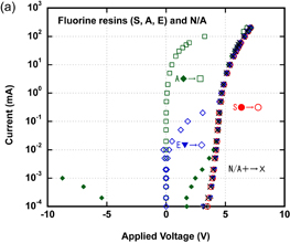
Download figure:
Standard image High-resolution image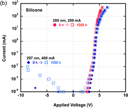
Fig. 7. (a) Marked increases in the leakage current observed for the fluorine resins except for S and N/A, corresponding to Fig. 6. On the other hand, the encapsulated samples using silicone do not show serious leakage at the side of the forward current (b).
Download figure:
Standard image High-resolution imageThe significant increase in leakage current for the underfilled and overcoated samples in cases A and E can be explained by molecular alignment and aggregation. It is reasonable to presume that a metal surface will attract the hydrophilic ends of the fluorine polymers. This is in agreement with the serious damage, resulting in a short circuit, which occurred within 95 h in the case of the –COOH polymer, earlier than that for the –COOCH3 polymer. When –OH groups accumulate on the surface of the metal, it is reasonable to expect serious damage to the electrode. On the other hand, the Si–O-based resin is considered to disperse H2O- and CO-related molecules in the bulk, even though these molecules are created by DUV-assisted polymerization.
4. Fabrication and demonstration of DUV LEDs with molded hemisphere encapsulation layers
Following the above detailed feasibility study, it is concluded that only the BVE-based fluorine with terminal –CF3 groups can be used for the encapsulation of DUV LEDs.16) Therefore, we decided to conduct endurance tests on encapsulated samples using the BVE-based fluorine resin with –CF3 ends. We prepared the encapsulated samples by placing a resin pellet on the die after it was underfilled and overcoated as shown in Fig. 8. Underfilling was carried out by the capillary action using a solvent and overcoating was performed by dripping the solution. Note that the encapsulation layers were naturally formed by the surface tension of the resin and encapsulation layers were not uniform. To recover the weak adhesive force of the fluorine resin to the surfaces of the AlN submount and die, anchor effects should be used; thus, the AlN submounts used in our experiments had a rough surface. In addition, the initial output power may differ among the dies. Thus, multiple samples were prepared for DUV irradiation with wavelengths of 265, 285, and 300 nm. To separate the degradation of the dies from that of the fluorine resin, we plot RLEE in Figs. 9(a)–9(c). When the difference in initial output power was canceled, RLEE was flat after the burn-in treatment of 100 h for the 265 nm samples. For the 285 nm samples, after the burn-in for 24 h, there were no obvious changes in RLEE and the bare dies maintained a constant output power during the endurance test. Similarly, for the 300 nm samples, the output power was reasonably stable without burn-in treatment. Note that 1 h in Fig. 9(c) corresponds to the initial output power at 0 h since a log scale was used on the x-axis. All results indicate no obvious degradation of the fluorine resin when the effect of the die degradation during the endurance test is removed. Thus, by extrapolating our results, the lifetime of the resin is considered to be much greater than 10,000 h.
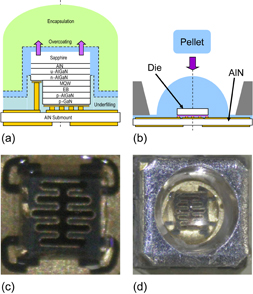
Fig. 8. (a) Schematic diagram of COB package and (b) encapsulation procedure of the samples, which involves placing a fluorine resin pellet on the die. (c) Photograph of typical sample with underfilling and overcoating. (d) Photograph of typical encapsulated sample.
Download figure:
Standard image High-resolution image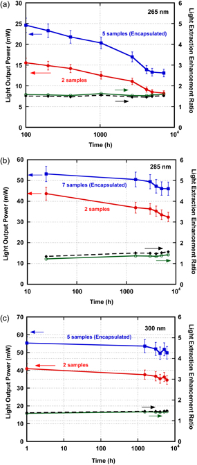
Fig. 9. Results of endurance tests focusing on the degradation of fluorine resin. To illustrate the changes in the resin, RLEE is shown as a function of the endurance time for samples irradiated with (a) 265, (b) 285, and (c) 300 nm DUV light to cancel the effect of the degradation of LED dies during the endurance test.
Download figure:
Standard image High-resolution imageSince the durability of the fluorine resin has been confirmed, mold encapsulation was attempted. Figure 10 shows the procedure used for the mold encapsulation and a photograph of a sample after encapsulation using a single concave hemisphere depression of 3 mm diameter. AlN submounts with sizes of 5 × 5 mm2 were prepared and the die size was 1.3 × 1.3 mm2. We fabricated two samples with RLEE values of 1.49 and 1.51, which are considered to be very stable owing to the mold. On the basis of these results, we attempted to fabricate an array of modules with encapsulated dies while bearing in mind the possibility of COB production on a ceramic sheet. The size of the four submounts was 3 × 9 mm2 and each submount included three locations for die mounting. After three 1.3 × 1.3 mm2 dies were placed on each submount, four submounts were placed with a gap of 0.2 mm between them on a patterned circuit board (PCB) with an isolation layer of diamond-like carbon (DLC) on a thin oxidized Al layer17) on a Duralumin panel of 1.5 mm thickness, which is durable against DUV light. Thus, twelve dies were connected in series on the DLC-PCB. After placing the 3 × 4 array of 285 nm LED bare dies on the DLC-PCB, the encapsulation procedure was performed using a single mold with 12 concave depressions. Figure 11(a) shows photographs of the encapsulated array module. Also, a photograph taken when a driving current of 200 mA was applied is shown. The weak emission of visible blue light is considered to be caused by the deep levels in the AlGaN active layer of our DUV LEDs, which may correspond to the yellow center of blue InGaN LEDs. This visible emission is negligible in comparison with the electroluminescence at 285 nm. Figure 12 shows the output power of the array module as a function of the forward current for the cases with and without encapsulation. RLEE was calculated to be 1.5, in good agreement with that in the single-die experiment. Despite the maximum current of 200 mA for our power supply, an output of 472 mW at 200 mA and 63 V was recorded. The current density at a mesa cross section was 30 A/cm2, but the maximum current density of our dies was thought to be greater than 100 A/cm2 from our numerous endurance tests. Therefore, we expect that the improvement of heat dissipation will realize an output power of W/cm2 at 100 A/cm2.
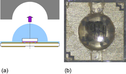
Fig. 10. (a) Schematic diagram of formation of hemispherical encapsulation layer by mold technique and (b) photograph of typical sample with the hemispherical encapsulation layer.
Download figure:
Standard image High-resolution image
Fig. 11. Photographs of the 285 nm LED array module. (a) Photograph of as-encapsulated module (right) and photograph of single die (left). (b) Photograph obtained when a driving current of 200 mA was applied.
Download figure:
Standard image High-resolution image
Fig. 12. Optical output power of the 3 × 4 array module as a function of forward current. The LED dies are connected in series.
Download figure:
Standard image High-resolution image
5. Conclusions
To add to the our works on the degradation mechanism of fluorine resins,4,13) we compared the feasibility of encapsulation with silicone resin and that with BVE-based fluorine polymers with –COOCH3 ends in comparison with fluorine polymers having terminal ends of –CF3 and –COOH. Except for the BVE-based polymer with –CF3 ends, serious damage to the electrode metal was observed. For the silicone resin, although the side chain of –CH3 was chosen to be robust against DUV light, the additional polymerization induced by DUV caused fatal cracks in the encapsulation layers, although the increase in leakage current was not maked. Including those used in our recent works, all the possible resins for the encapsulation of DUV LEDs were then compared. On the basis of the results, a BVE-based polymer with –CF3 ends was selected as an encapsulation material for DUV LEDs. During endurance tests on this resin, no obvious changes in the resin were observed. Following the above detailed feasibility study on the encapsulation materials, encapsulation with a hemispherical layer using a mold technique was attempted, and a stable RLEE of 1.5 was determined. Furthermore, a 3 × 4 array module of DUV LEDs was encapsulated simultaneously and an RLEE of 1.5 was also obtained, demonstrating the possibility of mass-producing COB packages. We believe that our results show the possibility of replacing mercury lamps and triggering a mercury-free age.