Arup Sarkar1* and K. A. Suresh2
1Department of Physics, Indian Institute of Science Education & Research, Berhampur 760010, Odisha, India
2Centre for Nano and Soft Matter Sciences, Prof. U R Rao Road, Jalahalli, Bangalore 560013, India
Corresponding Author E-mail: arupsarkar.katwa@gmail.com
DOI : http://dx.doi.org/10.13005/msri/170109
Article Publishing History
Article Received on : 15 March 2020
Article Accepted on : 10 April 2020
Article Published : 11 Apr 2020
Plagiarism Check: Yes
Reviewed by: Narendra Kumar Ahirwar
Second Review by: Subramanian Ravichandran
Final Approval by: Sami Mahmood
Article Metrics
ABSTRACT:
To realise the miniaturised devices, the precise measurement of nanoscale tunnelling current in ultrathin films is of utmost importance. For the nanoscale current measurements, current sensing atomic force microscope (CSAFM) is one of the most powerful tool. CSAFM allows to map the current distribution on the film surface and it permits to perform current measurements as a function of applied bias voltage. It has turned out to be crucial for studies of organic films. In CSAFM, a physical contact is made on film with a precise control of the applied force in nanonewton (nN) range. For the preparation of ultrathin film, Langmuir-Blodgett (LB) technique is known to provide a uniform film with a good control over the thickness in the molecular level. In the last two decades, there have been many CSAFM studies for the tunnelling current measurements. This review is intended to cover the literature on the tunnelling current measurements using CSAFM.
KEYWORDS:
Tunnelling Current; Ultrathin Film; Current Sensing Atomic Force Microscope; Negative Differential Resistance
Copy the following to cite this article:
Sarkar A, Suresh K. A. Tunnelling Current Measurements Using Current Sensing Atomic Force Microscope. Mat. Sci. Res. India; 17(1).
|
Copy the following to cite this URL:
Sarkar A, Suresh K. A. Tunnelling Current Measurements Using Current Sensing Atomic Force Microscope. Mat. Sci. Res. India; 17(1). Available from: https://bit.ly/2XsOzXa
|
Introduction
In the electronic devices, a great amount of energy is released in the form of Joule heat. This reduces the lifetime of the devices. To tackle this problem, one of the approach can be replacing these devices with quantum devices. Quantum devices work on the principles of quantum mechanics like quantum tunnelling, quantum entanglement and so on. Quantum tunnelling suggests that a particle with energy less than barrier height can penetrate the barrier. The probability of the tunnelling decays exponentially with the width of the barrier. Here, the width of the barrier corresponds to the film thickness. Hence, to attain a higher value of the tunnelling probability one needs films as thin as possible. In this context, ultrathin films whose thickness is typically less than 10 nm are very useful.1
To acquire ultrathin films, there are many techniques like spin coating, molecular beam epitaxy, atomic layer deposition and so forth. However, Langmuir-Blodgett (LB) technique is one of the most demanding technique. It provides films of uniform thickness with a good control over molecular orientation.2 Furthermore, it is possible to obtain multilayer film of various molecular architectures with controlled thickness.2 The only requirement for LB technique is that the molecules need to be amphiphilic i.e., it should have both hydrophilic and hydrophobic parts. Amphiphilic molecules floating at the air-water (A-W) interface to form a monolayer film is called Langmuir film. The Langmuir film can be compressed symmetrically to obtain different phases. This film at the A-W interface can be transferred onto solid substrate to get a uniform LB film of well-defined phase.
In recent times, many types of scanning probe microscope have emerged for nanoscale electrical measurements of sample. Current sensing atomic force microscope (CSAFM) is one of the most promising as it allows to correlate the electrical property with the surface topography with high spatial resolution. CSAFM is used in contact mode and it can give tip-sample junction properties. Here, the cantilever tip is coated with conducting film (usually with platinum) and the substrate is conducting in nature. Thus, they behave as top and bottom electrodes respectively. Applying a bias voltage across the films with the electrodes results in a current that is used for the spatially resolved current distribution imaging. The current distribution image is obtained at constant force of tip on the film. By varying the bias voltage, the contrast of the current image can be changed. For making top contact, it is possible to have control on the force in nanonewton (nN) scale. Further, it is possible to carry current-voltage characteristics studies. Also, it is suggested to use CSAFM when small surface feature is surrounded by the insulating area. In CSAFM, the tip positioning is decoupled from the electrical measurements, helping measurement of wide range of conductivity. For some cases, it is important to know the variation of electrical property as a function of load (force). In soft material like biological systems, applied force is known to be an important parameter for electrical conductivity studies. Force-dependent conductivity has been reported for azurin protein.3 Holo-azurin with the Cu redox group shows good stability in conductivity with increase in applied force, whereas apoazurin without Cu group has shown less stability.4 In the proteins, plastic deformation is a common issue with the applied force. It means there is deformation in conformation after some point of applied force. After that it does not revert to previous conformation. This leads to the variation of conductivity with the applied force. To investigate such variation of conductivity with the applied force, CSAFM is indispensable.
The intention of this review is to discuss the tunnelling current measurements in ultrathin films by using CSAFM. We first start to describe the basic understanding of the charge transport in the light of Simmons’ approach. Afterwards, recent advances in this field of research are reviewed.
Charge Transport Mechanism
There are different models such as hopping, tunnelling via superexchange, sequential tunnelling, flickering resonance model and so forth to describe the charge transport.5 When we have metal-insulator-metal (M-I-M) type of junctions, to analyse the charge transport through these junctions, Simmons’ equation has been a successful approach. Basically, this is applicable for ultrathin films where tunnelling is a dominant process. Simmons has given the following generalized equation for tunnelling through M-I-M junction6

Here, Ac is area of contact between sample surface and electrode, m* is effective electron mass, φ is mean barrier height, is mean barrier width, q is the electronic charge, h is the Planck’s constant and V is the applied voltage.
The barrier, at the low bias regime has rectangular shape and Eq. (1) yields
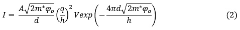
Here, φ0 is height of rectangular barrier and d is the distance between two electrodes.
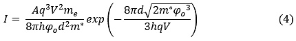
With the increase of applied bias voltage, the barrier changes from rectangular to trapezoidal shape and Eq. (1) reduces to

In this situation, tunneling happens from one electrode to another directly and this is called direct tunnelling.
With further increase in applied bias, the barrier shape changes from trapezoidal to triangular when the bias voltage is higher than the barrier height. Then, Eq. (1) becomes
Here, me is the electron rest mass. In this situation, electron from one electrode gets injected into insulator in first step and then the electron reaches to another electrode in next step. The whole process is called injection or Fowler-Nordheim tunnelling.
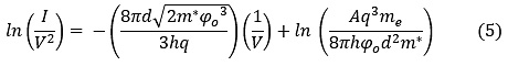
Thus, one has straight line in the plot of ln (I/V2) vs 1/V for injection tunneling mechanism. For direct tunneling mechanism, ln (I/V2) varies logarithmically with 1/V. The applied bias voltage, corresponding to the transition from direct to injection tunneling is called transition voltage (Vtrans).
Resonant tunnelling is another important mechanism for charge transport in ultrathin films. In this, molecular energy levels are used for tunnelling. It can lead to phenomenon like negative differential resistance (NDR) which has many technological applications. There are some reports discussing NDR in organic as well in inorganic systems.7-11 However, most of the reports are at low temperature. For device applications, it is desirable to get low values of NDR voltages. Hence, there has been interest on how to decrease the NDR voltages.
Discussion
Understanding the charge transport through tunnelling junctions is relevant for successful molecular electronic devices. In tunnel junctions, molecules or molecular film of monolayer thickness form the metal-molecules-metal junctions (a type of metal-insulator-metal junctions). In alkyl-based junctions the charge transport mechanism is reported to be direct tunnelling in the applied voltage range of 1 V.12 In alkyl systems, due to large (8 eV) highest occupied molecular orbital–lowest unoccupied molecular orbital (HOMO-LUMO) gaps, direct tunnelling is dominant mechanism when the applied bias voltage has less value than the barrier height. Direct tunnelling is a kind of non-resonant tunnelling. A decreased value of the HOMO-LUMO gap for the conjugated systems opens the possibility of other transport mechanisms like resonant tunnelling, electron hopping and so on. A transition was found from direct tunnelling to field emission at applied bias voltage (less than or equal to 1 V) for few π conjugated thiols.13 They have shown that gold-molecule-gold junctions formed of π-conjugated thiols gives current-voltage characteristic in accordance with a transition of a trapezoidal barrier to a triangular barrier at moderate applied bias voltage.13 These experiments were carried out using CSAFM. In these cases, Simmons equation was employed for the analysis and extraction of parameters like effective mass and barrier height which are useful for the tunnelling device applications. Similar kind of experiments were performed using CSAFM for ultrathin monolayer films (prepared by LB technique) of technological relevant molecules.
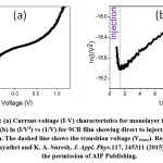
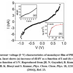
The room temperature liquid crystalline phases of n-alkyl cyanobiphenyls (nCBs) have made it suitable for the liquid crystal displays. Liquid crystalline phase possesses properties of both liquid and crystalline phases. Hence, there is a lot of interest in the research of nCBs since its synthesis.14 They are known to be surface active and can form Langmuir monolayer.15,16 Electrical conductivity studies (at optimized force) on the monolayer films of 9CB and 10CB were reported by using CSAFM.17 The monolayer films were prepared by using LB technique. In both cases highly oriented pyrolytic graphite (HOPG) was used as a bottom conducting substrate. They found tunnelling mechanism for the charge transport (Figure 1(a) shows for 9CB).17 They reported a transition from direct tunnelling to injection tunnelling with increase in applied voltage (Figure 1(b) shows for 9CB). The effective mass of electron was estimated to be 0.021 me and 0.065 me for 9CB and 10CB respectively.17 Also, they found the barrier height in 10CB for electron transport is lower compared to that in 9CB. Barrier height is obtained from the voltage corresponding to the transition point as shown by dashed line in Figure 1(b).17 This interesting behaviour was explained by the odd-even effect and the molecular interaction with the substrate.17 It is known that the molecules with even number of methylene groups possess lower barrier height than that with odd number of methylene groups.19 The odd-even effect is known to play vital roles for other physical properties too.19,20 For bioelectronics applications, understanding the charge transport mechanism through biomaterial is crucial. Charge transport studies in ultrathin films of ionic disk-shaped liquid-crystal molecules pyridinium tethered with hexaalkoxytriphenylene (PyTp) and its complex with DNA (PyTp-DNA) is reported.21 Fowler-Nordheim (FN) model was used to fit the I-V curves.21 This indicates that the transport occurs through injection tunnelling mechanism. The barrier height for PyTp-DNA complex film was three times higher than that of pure PyTp film. The barrier heights were 0.45 eV and 0.15 eV respectively.21 Recently, cholesterol monolayer on graphene oxide monolayer was investigated for charge transport.22 They found a transition from direct tunnelling to injection tunnelling at a voltage of 0.72 V. Parameters like barriers height and effective mass were estimated for this system to be 0.72 eV and 0.021 me. Charge transport in a liquid crystalline polymer, 2,6-dihydroxy-3,7,10,11-tetraalkoxytriphenylene (PHAT) is reported to occur through direct tunnelling mechanism (Figure 2).23 The analysis suggested that the barrier height was about 1.22 eV. In all these cases, physical adsorbed films have been used. Normally, the current density for the chemisorbed film is higher than that for physical adsorbed film.5 There is an interest in the dependence of resistance on the molecular length. Due to non-resonant tunnelling, an exponential dependence of the resistance on the length of the molecule is reported for the aromatic systems.24
Figure 1: (a) Current-voltage (I-V) characteristics for monolayer film of 9CB on HOPG. (b) ln (I/V2) vs (1/V) for 9CB film showing direct to injection tunnelling transition. The dashed line shows the transition voltage (Vtrans). Reproduced from [H. N. Gayathri and K. A. Suresh, J. Appl. Phys.117, 245311 (2015)], Ref. 17 with the permission of AIP Publishing.
Figure 2: Current−voltage (I−V) characteristics of monolayer film of PHAT on gold coated mica. Inset shows (a) increase of dI/dV as a function of I and (b) variation of ln(I/V2) as function of 1/V. Reproduced from [H. N. Gayathri, B. Kumar, K. A. Suresh, H. K. Bisoyi and S. Kumar, Phys. Chem. Chem. Phys. 18, 12101-12107 (2016)], Ref. 23.
Proteins (azurin, bacteriorhodopsin etc.) are promising for future bioelectronics. There is a requirement for understanding of charge transport in proteins. The cofactor in the proteins can affect the transport behaviour significantly.25,26 In solid state measurement, electron conductivities are reduced in the apo (redox is absent) form by one to two orders of magnitude compared to the holo-protein (redox is present).27 Removing the Fe from the heme group, does not affect electron transport (ETp) in Cytochrome C.28 Cofactors aid in superexchange-mediated tunnelling and biomolecule-electrode electronic coupling.29 ETp is affected under compressive and tensile stress.30 Force-dependent current–voltage investigation has shown that holo-azurin (Cu redox is present), shows higher stability with increase in force (until ~30 nN) than the protein, apo-azurin (Cu redox is absent).30 For protein bacteriorhodopsin, the junction conductance increases linearly in the applied force range of 3–10 nN reversibly.31 In applied forces greater than 10 nN, the protein exhibits an irreversible change in conductance with force due to structural deformations (i.e. plastic deformation).31 In general, the range of decay length constant is between 0.12–0.30 Å−1 as estimated for protein monolayers films.32 The decay length constant is obtained from an exponential equation where the current varies exponentially with the thickness of the film in ETp measurements.32
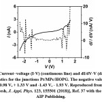
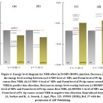
NDR is an important phenomenon having many technological applications like resonant tunnelling diode, oscillator and so on.33,34 Hence, there is a lot of interest in NDR research. In NDR, the current decreases with the increase in applied bias voltage, whereas in normal resistor the current increases with the increase in applied bias voltage. Noble laureate Leo Esaki has contributed a lot in this field for inorganic systems.9 Recently, there have been some studies on NDR in organic systems.35,36 NDR was found in ultrathin film of metal-phthalocyanine (MPc) on HOPG substrate (Figure 3).37 In current-voltage (I-V) curve, four dips correspond to the NDR. In dI/dV-V curve, negative values of dI/dV indicate NDR. The corresponding voltages (here, + 0.98 V, + 1.33 V and -1.43 V, – 1.93 V) are called NDR voltages (Figure3). The ultrathin film was prepared by using LB technique. In this technique, a film is deposited on solid substrate by vertical dipping of the substrate through the Langmuir film at A-W interface. It was argued that molecular resonant tunnelling to be the reason for NDR. Using the concept of resonance and off-resonance condition it was explained successfully. At positive applied bias voltage, when the Fermi level of Pt tip and LUMO level of MPc molecule are aligned in same level, there is increase in current due to resonance phenomenon.37 Further, increase in applied bias voltage creates an off-resonance condition between the Fermi level of platinum (Pt) tip and LUMO level of molecule (Figure 4(a)). This causes a fall in the current value.37 With further increase in voltage there will be resonance and off-resonance situation where the LUMO+1 level takes part to cause second NDR (Figure 4(b)). Similarly, in negative applied bias voltages, HOMO and HOMO-1 levels cause NDR (Figure 4(c) and (d)). All this was possible because of the very thin nature of the film. Other important aspect is NDR voltage value which is relevant to device applications. Graphene oxide is found to reduce the NDR voltage values behaving as hole dopant.37
Current-voltage measurements were carried out on Pd(II) alkanethiolate nanostructures (of bilayer thickness) for hexyl to hexadecyl by using CSAFM.38 They have reported the NDR effect due to Pd–S charge transfer mechanism. Also, they found that the resistance in the lower current region changes exponentially with the thickness (indicating a non-resonant tunnelling) giving a decay parameter value of about 0.2 Å−1.
Figure 3: Current−voltage (I-V) (continuous line) and dI/dV-V (dashed line) characteristics for the junctions Pt/MPc/HOPG. The negative value of dI/dV occurs at + 0.98 V, + 1.33 V and -1.43 V, – 1.93 V. Reproduced from [A. Sarkar and K. A. Suresh, J. Appl. Phys. 123, 155501 (2018)], Ref. 37 with the permission of AIP Publishing.
Figure 4: Energy level diagram for NDR effect in Pt/MPc/HOPG junction. Decrease in the energy level overlap between (a) LUMO level of MPc and Fermi level of Pt tip causes first NDR, (b) LUMO+1 level of MPc and Fermi level of Pt tip causes second NDR in positive bias direction. Decrease in energy level overlap between (c) HOMO level of MPc and Fermi level of Pt tip causes first NDR, (d) HOMO-1 level of MPc and Fermi level of Pt tip causes second NDR in negative bias direction. Reproduced from [A. Sarkar and K. A. Suresh, J. Appl. Phys. 123, 155501 (2018)], Ref. 37 with the permission of AIP Publishing.
Conclusions
In summary, we have discussed the studies on tunnelling current measurements performed by CSAFM. The thickness of the film or tunnelling path length was less than 10 nm. For understanding the tunnelling current, Simmons’ equation was reviewed. Barrier height and effective mass of electron, obtained from Simmons’ equation are discussed for films of 9CB, 10CB, PyTP, PyTP-DNA, PHAT etc. Charge transport through proteins is reviewed. The importance of applied force (by AFM tip on proteins) is described for charge transport studies. Also, decay parameter for non-resonant tunnelling is mentioned for different systems. Some reports on NDR phenomenon are described. It was explained that how molecular resonant tunnelling can lead to NDR in ultrathin film of MPc. At the end, it can be envisioned that the knowledge of tunnelling current will be very useful for the miniaturised device applications.
Acknowledgements
Arup Sarkar would like to thank Indian Institute of Science Education & Research Berhampur, for the Postdoctoral Research Fellowship.
Funding Source
This research received no specific grant from any funding agency.
Conflict of Interest
The authors have no conflicts of interest to disclose.
References
- K. Leosson, A. S. Ingason, B. Agnarsson, A. Kossoy, S. Olafsson and M. C. Gather,Ultra-thin gold films on transparent polymers.Nanophotonics2(1), 3-11 (2013).
- G. Roberts, Langmuir-Blodgett Films (Springer US, 1990), ISBN: 978-0-306-43316-0.
- J. Zhao, J. J. Davis, M. S. P. Sansom and A. Hung, Exploring the electronic and mechanical properties of protein using conducting atomic force microscopy.J. Am. Chem. Soc. 126, 5601-5609 (2004).
- W. Li,L.Sepunaru, N.Amdursky, S. R. Cohen, I.Pecht, M. Sheves and D.Cahen, Temperature and force dependence of nanoscale electron transport via the Cu protein azurin.ACS Nano 6, 10816-10824 (2012).
- C. D.Bostick, S.Mukhopadhyay, I.Pecht, M.Sheves, D.Cahen and D. Lederman, Protein bioelectronics: A review of what we do and do not know. Rep. Prog. Phys. 81(2), 026601 (1-57) (2018).
- J. G. Simmons, Generalized formula for the electric tunnel effect between similar electrodes separated by a thin insulating film. J. Appl. Phys.34(6), 1793-1803 (1963).
- B. Xu and Y. Dubi, Negative differential conductance in molecular junctions: an overview of experiment and theory. J. Phys. Condens. Matter 27 (26), 263202 (1-9) (2015).
- S. J. Molen and P. Liljeroth, Charge transport through molecular switches. J. Phys. Condens. Matter 22, 133001(1-30) (2010).
- L. L. Chang, L. Esaki and R. Tsu, Resonant tunneling in semiconductor double barriers. Appl. Phys. Lett. 24, 593-595 (1974).
- J. Jeon, M. J. Kim, G. Shin, M. Lee, Y. J. Kim, B. S. Kim, Y. Lee, J. H. Cho and S. Lee, Functionalized organic material platform for realization of ternary logic circuit, ACS Appl. Mater. Interfaces 12 (5), 6119-6126 (2020).
- S. Zhu, B. Sun, S. Ranjan, X. Zhu, G. Zhou, H. Zhao, S. Mao, H. Wang, Y. Zhao and G. Fu, Mechanism analysis of a flexible organic memristive memory with capacitance effect and negative differential resistance state, APL Mater. 7, 081117 (1-7) (2019).
- W. Wang, T. Lee and M. A. Reed, Mechanism of electron conduction in self-assembled alkanethiol monolayer devices. Phys. Rev. B 68, 035416 (1-7) (2003).
- J. M. Beebe, B. Kim, J. W. Gadzuk, C. D. Frisbie and J. G. Kushmerick, Transition from direct tunneling to field emission in metal-molecule-metal junctions. Phys. Rev. Lett. 97, 026801 (1-4) (2006).
- G. W. Gray, K. J. Harrison and J. A. Nash, New family of nematic liquid crystals for displays. Electron. Lett. 9(6), 130-131 (1973).
- J. Xue, C. S. Jung and M. W. Kim, Phase transitions of liquid-crystal films on an air-water interface. Phys. Rev. Lett. 69(3), 474-477 (1992).
- K. A. Suresh and A. Bhattacharyya, Formation of liquid crystalline phases from a Langmuir monolayer. Langmuir 13, 1377-1380 (1997).
- H. N. Gayathri and K. A. Suresh, Electrical conductivity in Langmuir-Blodgett films of n-alkyl cyanobiphenyls using current sensing atomic force microscope. J. Appl. Phys. 117, 245311(1-7) (2015).
- T. Toledano, H. Sazan, S. Mukhopadhyay, H. Alon, K. Lerman, T. Bendikov, D. T. Major, C. N. Sukenik, A. Vilan, and D. Cahen, Odd–Even effect in molecular electronic transport via an aromatic ring. Langmuir 30, 13596-13605 (2014).
- Y. Feng, E. R. Dionne, V.Toader, G. Beaudoin and A.Badia, Odd−Even effects in electroactive self-assembled monolayers investigated by electrochemical surface plasmon resonance and impedance spectroscopy. J. Phys. Chem. C 121, 24626-24640 (2017).
- L. Ramin and A.Jabbarzadeh, Odd-Even effects on the structure, stability, and phase transition of alkanethiolself-sssembled monolayers. Langmuir 27, 16, 9748-9759 (2011).
- A. Nayak and K. A. Suresh,Conductivity of Langmuir-Blodgett films of a disk-shaped liquid-crystalline molecule–DNA complex studied by current-sensing atomic force microscopy. Phys. Rev. E 78, 021606 (1-8) (2008).
- A. Sarkar, K. A. Suresh, H. N.Gayathri,Charge transport in a system of cholesterol molecules deposited on graphene oxide using current sensing atomic force microscope. Materials Today: Proceedings 11, 645-650 (2019).
- H. N. Gayathri, B. Kumar, K. A. Suresh, H. K. Bisoyi and S. Kumar, Charge transport in a liquid crystalline triphenylene polymer monolayer at air–solid interface. Phys. Chem. Chem. Phys. 18, 12101-12107 (2016).
- B. Kim, J. M. Beebe, Y. Jun, X. Y. Zhu and C. D. Frisbie, Correlation between HOMO alignment and contact resistance in molecular junctions: Aromatic thiols versus aromatic isocyanides. J. Am. Chem. Soc. 128, 4970-4971 (2006).
- S. Bera, J. Kolay, S. Banerjee, R. Mukhopadhyay, Nanoscale On-silico electron transport via ferritins, Langmuir 33 (8) 1951-1958 (2017).
- S. Bera, J. Kolay, P. Pramanik, A. Bhattacharyya and R. Mukhopadhyay, Long-range solid-state electron transport through ferritin multilayers, J. Mater. Chem. C 7, 9038-9048 (2019).
- S. Raichlin, I. Pecht, M. Sheves and D. Cahen, Protein electronic conductors: hemin–substrate bonding dictates transport mechanism and efficiency across myoglobin.Angew. Chem., Int. Ed. 54, 12379-12383 (2015).
- N. Amdursky, D. Ferber D, I. Pecht, M. Sheves and D. Cahen, Redox activity distinguishes solid-state electron transport from solution-based electron transfer in a natural and artificial protein: Cytochrome C and hemin-doped human serum albumin.Phys. Chem. Chem. Phys. 15, 17142-17149 (2013).
- L. Sepunaru, I. Pecht, M. Sheves and D. Cahen, Solid-state electron transport across azurin: from a temperature independent to a temperature-activated mechanism. J. Am. Chem. Soc. 133, 2421-2423 (2011).
- J. J. Davis, N. Wang, A. Morgan, T. Zhang and J. Zhao, Metalloprotein tunnel junctions: compressional modulation of barrier height and transport mechanism. Faraday Discuss. 131, 167-179 (2006).
- S. Mukhopadhyay, S. R. Cohen, D.Marchak, N. Friedman, I.Pecht,M.Sheves, and D.Cahen,Nanoscale electron transport and photodynamics enhancement in lipid-depleted bacteriorhodopsin monomers.ACS Nano 8, 7714-7722 (2014).
- I. Ron,L.Sepunaru, S. Itzhakov, T. Belenkova, N. Friedman, I.Pecht, M.Sheves, and D.Cahen, Proteins as electronic materials: electron transport through solid-state protein monolayer junctions. J. Am. Chem. Soc. 132, 4131-4140 (2010).
- X. Ran, P. Hou, J. Song, H. Song, X. Zhong and J. Wang, Negative differential resistance effect in resistive switching devices based on h-LuFeO3/CoFe2O4 heterojunctions, Phys. Chem. Chem. Phys. 22, 5819-5825 (2020).
- G. A. Gibson, Designing negative differential resistance devices based on self-heating, Adv. Funct. Mater 28 (22), 1704175 (1-9) (2018).
- Y. Majima, D. Ogawa, M. Iwamoto, Y. Azuma, E. Tsurumaki and A. Osuka, Negative differential resistance by molecular resonant tunneling between neutral tribenzosubporphine anchored to a Au (111) surface and tribenzosubporphine cation adsorbed on to a tungsten tip. J. Am. Chem. Soc.135 (38), 14159-14166 (2013).
- S. Rathi, S. K. Gupta, C. M. S. Negi and A. Singh, Negative differential resistance in heterojunction polymeric films. SuperlatticesMicrostruct.114, 15-22 (2018).
- A. Sarkar and K. A. Suresh, Negative differential resistance in nickel octabutoxyphthalocyanine and nickel octabutoxyphthalocyanine/ graphene oxide ultrathin films. J. Appl. Phys.123(15), 155501-15550 (1-7) (2018).
- N. S. John, S. K. Pati and G. U. Kulkarni, Electrical characteristics of layered palladium alkanethiolates by conducting atomic force microscopy. Appl. Phys. Lett.92(1), 013120 (1-3) (2008).

This work is licensed under a Creative Commons Attribution 4.0 International License.