
Abstract
Schottky diodes based on Al/polyaniline (PANI), electrodeposited by cyclic voltammetry (CV) with two different upper oxidation potentials, 0.8 and 1.1 V, respectively, were fabricated. Auger electron spectroscopy (AES) confirms the presence of hydrolysis products of PANI, benzoquinone (BQ)/hydroquinone (HQ) for PANI film deposited with a switch potential of 1.1 V. The electrical properties of the Al/PANI (with inbuilt hydrolysis products) and Al/PANI (without hydrolysis products) junctions were evaluated at different temperatures by current-voltage characteristics and impedance spectroscopy measurements. The presence of inbuilt hydrolysis products with PANI influences the electrical properties of the junction. The junctions were found to be rectifying in both cases but with wide differences in junction parameters, such as barrier height, ideality factor, and saturation current density, between them. The temperature dependence of the impedance spectra of the devices was found to have variations. Impedance parameters of the devices were deduced from a proposed equivalent circuit. The combined analyses of current-voltage characteristics and impedance measurements reveal that the presence of hydrolysis products with PANI in Al/PANI junction increases the contact resistance, depletion layer thickness, and barrier height of the device. © 2004 The Electrochemical Society. All rights reserved.
Export citation and abstract BibTeX RIS
Semiconducting conjugated polymers can be easily synthesized and obtained in the form of thin films suitable for device fabrication. Various conducting polymers such as polypyrrole, polythiophene, poly(3,4-ethylenedioxythiophene), and semiconducting polyaniline (PANI) are used in molecular electronic devices.1 2 3 4 The striking feature of PANI is that its electronic properties can be altered by chemical modifications, which provide significant effects on its physical properties. This feature coupled with a high degree of chemical stability in air makes PANI very attractive for a wide range of potential applications. Fabrication of solid-state heterojunction/Schottky devices is one of the most important applications for PANI.
Schottky devices have been successfully fabricated with metal and semiconducting polymers5 6 7 8 and the electronic properties controlling the device performance, such as rectifying ratio, barrier height, and work function, have been evaluated through measurements of dark current density against applied voltage. Generally, metals possessing a high work function, such as Au, give ohmic contacts, while metals possessing a low work function, such as Al, provide rectifying contacts. The barrier generated at the metal/polymer interface creates an environment for blocking charge carriers. The efficiency of the device is predominately determined by the injection efficiency of the minority carriers surmounting the barrier. Hence, the physical and chemical states of the polymer, which is used for establishing contact, are the determining factors that influence the efficiency of the device.
A few interesting studies have been directed on the possible chemical interaction between metal and polymer at the interface.4
9 The dopants present in the conjugated polymer contribute to the chemical interaction with metal and result in an insulating layer on the metal surface. The electrical properties of metal contacts with doped polypyrrole,9 with polymeric anions, and doped poly[3-(4-octylphenyl)-2,2'-bithiophene]10 with  were analyzed in terms of insulating film formation. Also, chemistry-induced defects formed when metal atoms are deposited on the conjugated polymer surface are known to alter electronic properties of the devices.11
12 Dannetun et al.13 have reported that aluminum atoms evaporated on the surface of poly(3-octylthiophene) films react with active groups in polymer chains to result in a complex. In a similar way, Lachkar et al.14 reported sulfide-like complex formation at the interface with metals like Cu and Ag as a result of interactions between the semiconducting conjugated poly(3-hexylthiophene) and the metal.
were analyzed in terms of insulating film formation. Also, chemistry-induced defects formed when metal atoms are deposited on the conjugated polymer surface are known to alter electronic properties of the devices.11
12 Dannetun et al.13 have reported that aluminum atoms evaporated on the surface of poly(3-octylthiophene) films react with active groups in polymer chains to result in a complex. In a similar way, Lachkar et al.14 reported sulfide-like complex formation at the interface with metals like Cu and Ag as a result of interactions between the semiconducting conjugated poly(3-hexylthiophene) and the metal.
Hence, it becomes imperative to note that chemistry-induced defects formed at the interface between a semiconducting conjugated polymer and a metal can play a crucial role in deciding junction properties. For instance, a peculiar symmetrical but nonohmic behavior has been noticed in the sandwich device, Al/doped poly(3,4-ethylenedioxythiophene)/indium-tin-oxide (ITO).4 However, the research has not been extended for any of such device with PANI as the semiconducuting polymer. This might be due to the absence of any complex forming groups in PANI with the contact metal.
Recently, our reports demonstrated that in situ induced hydrolysis products of PANI, the BQ/HQ redox pair, significantly alter the impedance characteristics of PANI embedded with BQ/HQ.15 16 17 It would be interesting to evaluate the junction properties of the electronic device fabricated with PANI having the induced hydrolysis products in it.
In the present study, we report the electrical features of junctions between a metal and electrochemically polymerized PANI in the doped form with incorporated BQ/HQ inbuilt in the PANI matrix. The influence of BQ/HQ on the Schottky barrier developed with Al and PANI(BQ/HQ) was further investigated. The Schottky diodes were fabricated by using Au whose work function is 4.8 eV higher than that of PANI (which lies between 4.1 and 4.28 eV18) to form an ohmic contact with PANI, while on the other side, aluminum possessing a low work function of 3.7 eV was used to make a rectifying contact with PANI. The measurements of current-voltage and ac impedance were conducted to bring out the influence of in situ generated hydrolysis products on junction properties of Schottky diodes. PANI films were electrodeposited in different conductions by cyclic voltammetry and used for this purpose.
Experimental
Chemicals.—
Reagent grade aniline (Merck) was doubly distilled, and the resulting colorless liquid was kept under nitrogen in the dark at 5°C. All other reagents were Merck or GR samples and used without pretreatment.
Electrodeposition of PANI with or without hydrolysis products.—
Electrochemical deposition of PANI was made by using the Autolab PGSTAT 30 (Eco. Chemie B.V., The Netherlands) with a general purpose electrochemical system software. A three-electrode cell assembly was utilized with an Ag/AgCl reference electrode (Argenthal, 3 M KCl, 207 mV vs. SHE at 25°C). Platinum wire was used as the counter electrode. A gold foil of area 1 cm2 was used as the working electrode. A Luggin capillary, whose tip was set at a distance of about 1 mm from the surface of the working electrode was used to minimize errors due to  drop in the electrolytes. The deposition of PANI was performed under nitrogen atmosphere.
PANI films were electrochemically deposited in a 1 M HCl solution with 100 mM aniline by using cyclic voltammetry (CV) under two different conditions. The upper potential limit was set as 0.8 or 1.1 V in the cyclic voltammetry with a scan rate of 50 mV/s. PANI deposition with the upper potential limit of 1.1 V resulted in in situ hydrolysis products.19 20 The deposited PANI films were designated as PANI-a and PANI-b to denote PANI without and with hydrolysis products, respectively.
PANI films were dried at 100°C for 1 h and then kept under vacuum for 2 days to remove the entrapped moisture from the polymer matrix and then used for further measurements.
Auger electron spectroscopy.—
Auger electron spectroscopy (AES) measurements of PANI films were performed with ESCA 210 and MICROLAB 310D (VG Scientific Ltd., UK) spectrometers. AES depth profiling was conducted at emission currents of 0.1 and 8 mA with gun tensions of 10 (electrons) and 3 kV (ions), respectively.
Schottky diodes with PANI.—
Approximately 100 nm thick strips of aluminum were vacuum evaporated at a pressure of  Torr to have metal contact with PANI. The active area of the metal/polymer contact was 0.28 cm2. The fabricated devices of Au/PANI-a/Al and Au/PANI-b/Al are denoted as device a and device b, respectively. Such a sandwich structure was used for current-voltage and ac impedance measurements.
Current-voltage and ac impedance measurements.—
Current-voltage characteristics were measured using model 2400 series SourceMeter (Keithley, USA) and scanned in the potential range between −1.3 and +1.3 V. The impedance spectrum analyzer, IM6 (ZAHNER, Germany), with Thales software was employed to measure and analyze the ac impedance spectra. The potential amplitude of ac was kept as 10 mV and its frequency range was used from 1 MHz to 500 Hz. AC impedance measurements were made at different applied dc voltages.
Results and Discussion
Preparation of PANI film with builtin hydrolysis products.—
Electrodeposition of PANI was performed by cyclic voltammetry (CV) at two different switching upper potentials, 0.8 and 1.1 V, respectively, to make PANI films, PANI-a and PANI-b, without and with hydrolysis products. CVs (Fig. 1) recorded with concomitant deposition of PANI with these two conditions clearly reveal the presence of BQ in PANI-b film deposited with the upper potential of 1.1 V. It is expected that electrodeposition of PANI by cyclic voltammetry with a switching  V, could result in BQ as the hydrolysis product.19
20
21
22 In Fig. 1b, besides the characteristic peak at 0.25 V for the conversion of leucoemeraldine to emeraldine (polaronic radical cation) form of PANI, a peak at 0.60 V for the oxidation of head-to-tail dimer, and the peak at 0.80 V for the generation of diradical dications in the PANI structure, the presence of a peak at 0.50 V indicates the formation of a degradation product of PANI, BQ. Kobayashi et al.19 and Stilwell and Park20 assigned the peak around 0.50 V during PANI growth for the generation of BQ. Several other researchers have also reported the formation of BQ as the hydrolysis product during PANI deposition.23
24 Consecutive reactions involving the hydrolysis of the quinoid site of PANI (emeraldine form) and the formation of a p-aminophenol type intermediate via an electrochemical electron transfer followed by a chemical reaction25 result in BQ. Reduced PANI with a shorter chain length can be a result of this process.
V, could result in BQ as the hydrolysis product.19
20
21
22 In Fig. 1b, besides the characteristic peak at 0.25 V for the conversion of leucoemeraldine to emeraldine (polaronic radical cation) form of PANI, a peak at 0.60 V for the oxidation of head-to-tail dimer, and the peak at 0.80 V for the generation of diradical dications in the PANI structure, the presence of a peak at 0.50 V indicates the formation of a degradation product of PANI, BQ. Kobayashi et al.19 and Stilwell and Park20 assigned the peak around 0.50 V during PANI growth for the generation of BQ. Several other researchers have also reported the formation of BQ as the hydrolysis product during PANI deposition.23
24 Consecutive reactions involving the hydrolysis of the quinoid site of PANI (emeraldine form) and the formation of a p-aminophenol type intermediate via an electrochemical electron transfer followed by a chemical reaction25 result in BQ. Reduced PANI with a shorter chain length can be a result of this process.
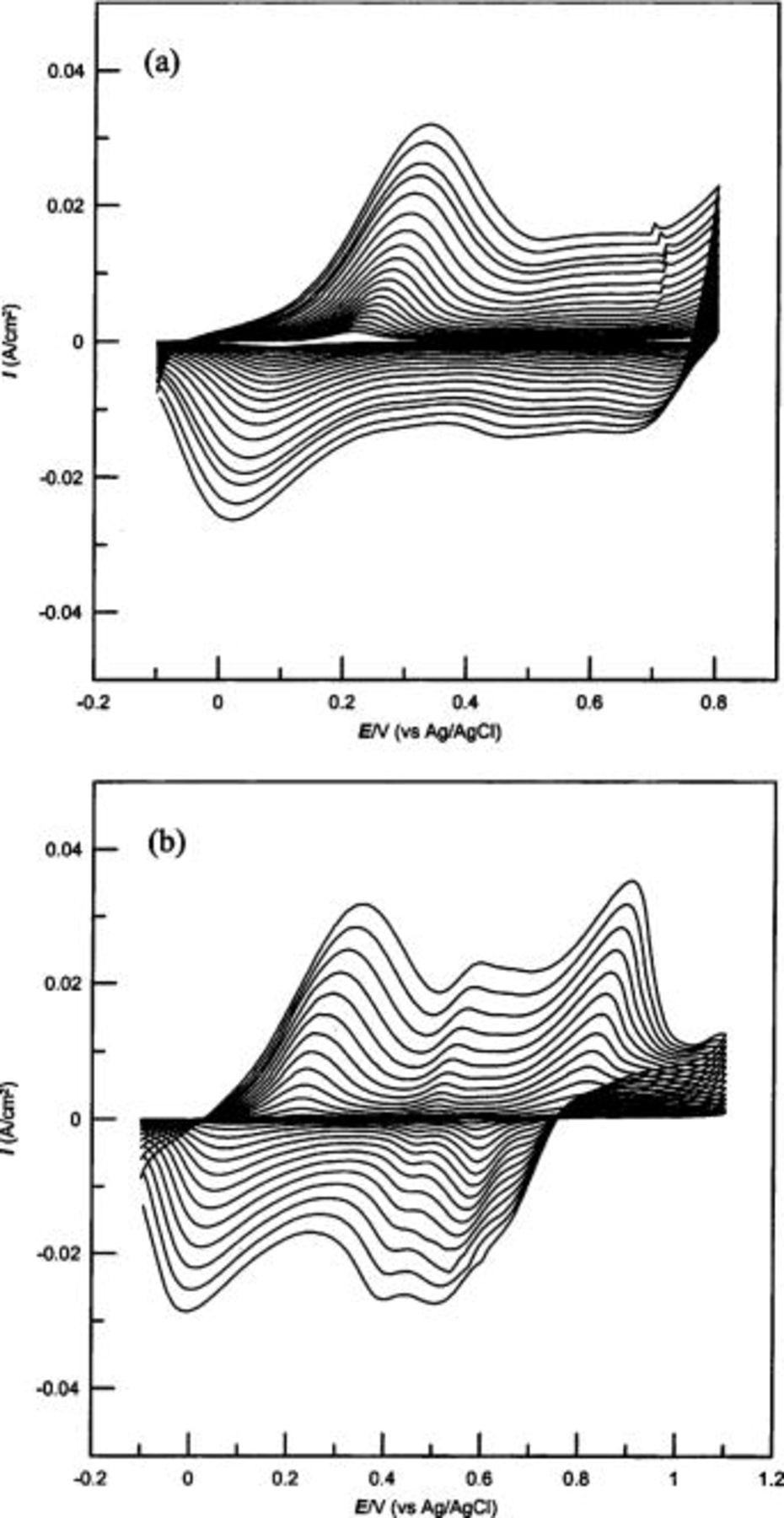
Figure 1. CVs of growth of PANI films on gold electrodes with the upper potential limits of (a) 0.8 V (PANI-a) and (b) 1.1 V (PANI-b).
In contrast to Fig. 1b, the peak representing BQ formation was not obvious when PANI-a was deposited with the upper potential limit of 0.80 V (Fig. 1a), informing a negligible proportion of BQ generation during deposition of PANI-a.
Our aim is to study and compare the electronic and junction properties of these two PANI films with Al as the contact metal. Hence, film thicknesses of these two films were controlled so as to be close to each other. The thickness (d) of the deposited PANI films was estimated from the charge necessary to convert the leucoemeraldine form of PANI to the emeraldine form (using the area under the first redox process in the voltammograms).26 27 The following equation was used to calculate the thickness of films
where Q is the charge under the first cyclic voltammetric peak;  the molecular weight of aniline (93.13 g mol−1);
  (number of electrons/aniline unit); A the area of the electrode (1.0 cm2); ρ the specific density of aniline (1.02 g cm−3), and F is the Faraday constant. The thickness of films were estimated as 1.7 and 1.8 μm for PANI-a and PANI-b, respectively. Thus, the two films deposited at the two different conditions were controlled so as to have a similar thickness.
Auger profile of oxygen concentration in PANI films.—
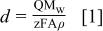
The inclusion of BQ in PANI-b was confirmed by Auger electron spectroscopy (AES). Spectra of PANI-a and PANI-b were recorded to ascertain the presence of builtin BQ in the bulk of polymer films. The depth profiles of the O signal were compared (Fig. 2) and found that PANI-b has a higher proportion of BQ in the film. Previously, X-ray photoelectron spectroscopy (XPS) was used to obtain such information.15 16 The Auger profile of PANI-b clearly shows the existence of BQ in the film. The observed higher concentration of O at the surface is probably due to the migration of BQ from the bulk of the polymer to the surface during the film drying process.
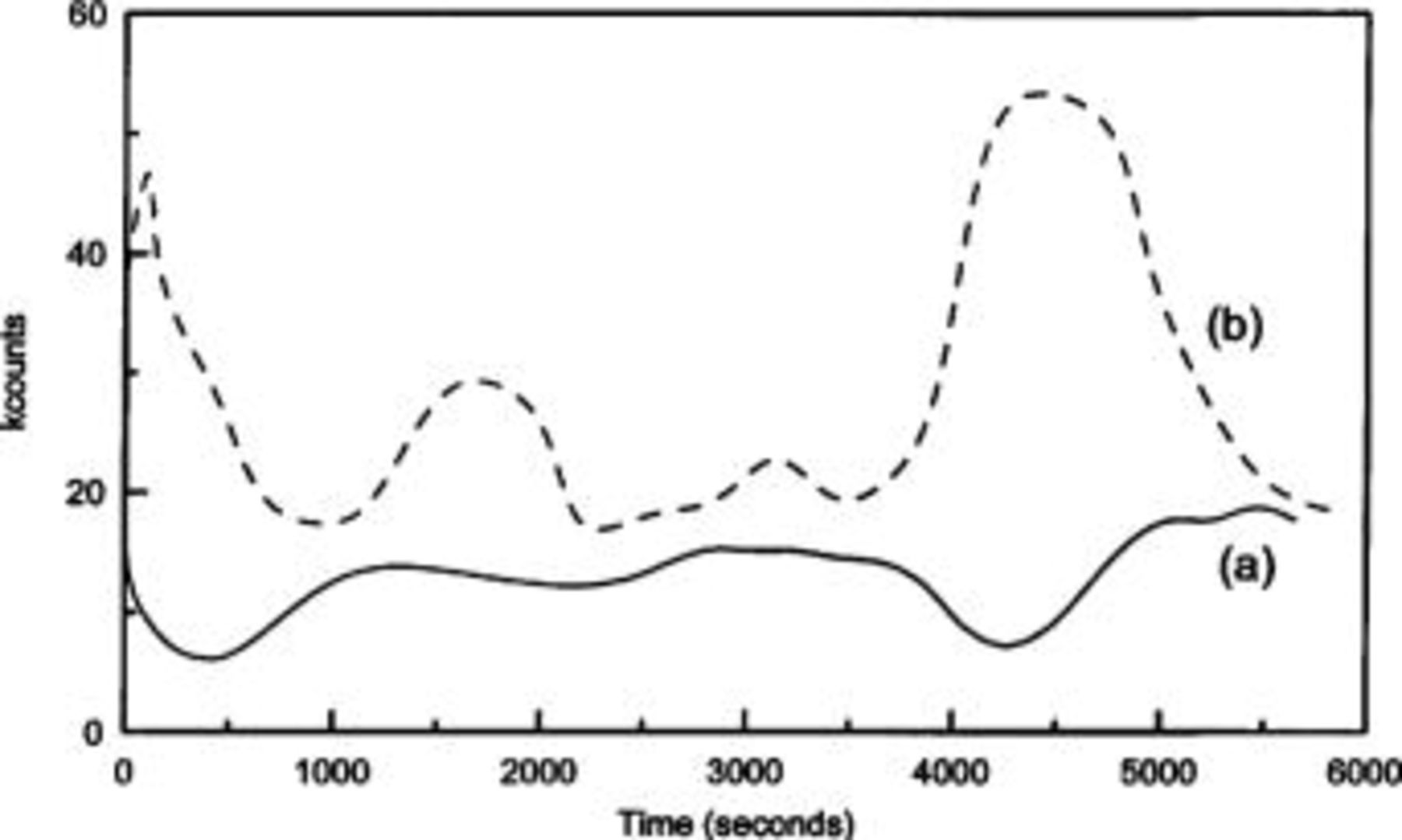
Figure 2. The Auger depth profiles of O element from (a) PANI-a and (b) PANI-b films.
Electronic properties of the Schottky barrier.—
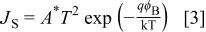
Schottky barrier devices were fabricated independently with these two PANI films in the sandwich configuration, Au/PANI-a/Al (device a) and Au/PANI-b/Al (device b). Figure 3 shows typical current density vs. voltage  characteristics of these devices at various temperatures. The
  relation for both devices is asymmetrical and rectifying. Striking differences in the
  characteristics between the two devices were observed, and these are attributed to the presence of BQ in PANI film. The
  curves for different temperatures of device b are close to each other and have low current densities (less than 2.5 mA/cm2). In contrast, device a shows temperature dependent
  curves. This indicates that the carrier transport in metal/semiconductor contacts are different between these devices.
Figure 3. Temperature dependence of current density vs. applied voltage  rectification characteristics for (a) Au/PANI-a/Al and (b) Au/PANI-b/Al devices.
The transport of charge from the semiconductor over the potential barrier into the metal could be described by the thermionic emission theory or the diffusion theory of metal/semiconductor rectification.28
The current density (Fig. 3) could be explained by using Richardson's equation expressed as
where  is the saturation current density,
  the applied potential, q the electronic charge, n the ideality factor, k the Boltzmann constant, and T is the absolute temperature. The saturation current density is defined as
where  is the Richardson constant (=120 A K−2 cm−2 for a free electron), and
  is the barrier height at the metal/semiconductor interface.
The  vs.
vs.  plots of device a and b at different temperatures are given in Fig. 4a and b, respectively. The values of
  and n were calculated for different temperatures from the intercept and slope of the linear region of
  vs.
vs.  plots, and are listed in Table I. Furthermore, the values of barrier height (obtained according to Eq. 3) and rectification ratio (at ±0.7 V) are also presented in Table I.
Figure 4. Temperature dependence of  vs.
vs.  characteristics of the junctions for (a) Au/PANI-a/Al and (b) Au/PANI-b/Al devices.
Table I.
| Electronic parameters of Schottky junctions for the devices. | |||||
|---|---|---|---|---|---|
| Device | Temperature(°C) | Saturation current density
 (A/cm2) (A/cm2) | Ideality factor n | Barrier height
 (V) (V) | Rectification ratio r (at 0.7 V) |
| Au/PANI-a/Al (device a) | 5 |
 | 12.53 | 0.81 | 72.44 |
| 25 |
 | 14.76 | 0.62 | 20.89 | |
| 45 |
 | 11.77 | 0.66 | 18.62 | |
| 65 |
 | 10.31 | 0.69 | 57.54 | |
| Au/PANI-b/Al (device b) | 5 |
 | 13.91 | 0.64 | 0.85 |
| 25 |
 | 10.64 | 0.69 | 0.91 | |
| 45 |
 | 9.31 | 0.74 | 0.95 | |
| 65 |
 | 8.87 | 0.79 | 1.23 | |
Large values of the ideality factor of device a (∼10-15) and b (∼8-14) were obtained (Table I), and these results are in agreement with that of polypyrrole/metal Schottky device3 for which the ideality factor was reported as 10. The higher values of n noticed for the conducting polymers are due to the fact that these polymers are present in the form of aggregates of primary and secondary particles, irrespective of polymerization conditions. Accordingly, two different electron transport mechanisms are feasible.29 Additionally, the substantial departure from the value of unity for the ideality factor may be attributed to the doped nature of PANI with a high concentration of dopant, and/or the recombination in the depletion region.8 30
 of device b is found to be higher than device a. The higher
  and lower
  (at any temperature ⩾25°C) for device b are expected to arise from the difference in the metal/PANI interfacial characteristics between the two devices. It is important to note that PANI in device b has inbuilt BQ in contrast to device a. Hence, the presence of in situ generated BQ is expected to alter the metal/PANI interfacial characteristics.
Earlier reports on the sandwich structure of the reactive metal/doped polymer/Au, reveal the formation of a thin interfacial insulating film between the deposited metal atoms and the conducing polymer as a result of the chemical reaction.11 The formation of an insulating film is supposed to occur via the reaction of the oxygen groups in the dopant/polymer with metal. The dioxoethylene bridge present in poly(3,4-ethylenedioxythiophene) (PEDOT) interacts with aluminum to result in an insulating layer.4 As a consequence of the insulating layer, π bands of conducting polymers are expected to be affected. Also, the interfacial layer can induce reorientations of the molecular backbones.31 In the present study, the coexistence of BQ with PANI in device b may hasten interaction with Al and the subsequent changes in interfacial characteristics can be inferred from ac impedance studies on the interface.
AC impedance analyses.—
To get more insight into the interfacial characteristics at Al/PANI junction, ac impedance measurements of device a and b were independently performed as functions of temperature and bias voltages. Figure 5 and 6 display the impedance behavior of device a and b at different temperatures and bias voltages, respectively. It is indicated from Fig. 5 and 6 that there are differences in the impedance behavior between these two devices. The temperature response of impedance (Fig. 5) for these devices is similar to  characteristics (Fig. 2). Device b shows a lower temperature dependence on impedance than device a. This indicates that the observed differences in
  characteristics and impedance may have the same origin. The reason for such differences is analyzed in terms of the presence of BQ in device b in contrast to device a. The impedance parameters are deduced from a proposed equivalent circuit (Fig. 5a, insert).
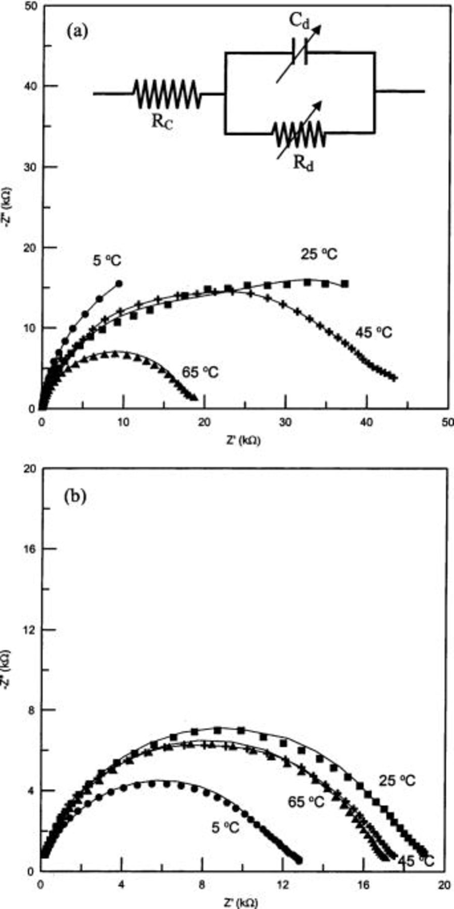
Figure 5. Temperature dependence on Nyquist diagrams for (a) Au/PANI-a/Al and (b) Au/PANI-b/Al devices at the applied bias potential of 0 V. Inset in (a) is the corresponding equivalent circuit.
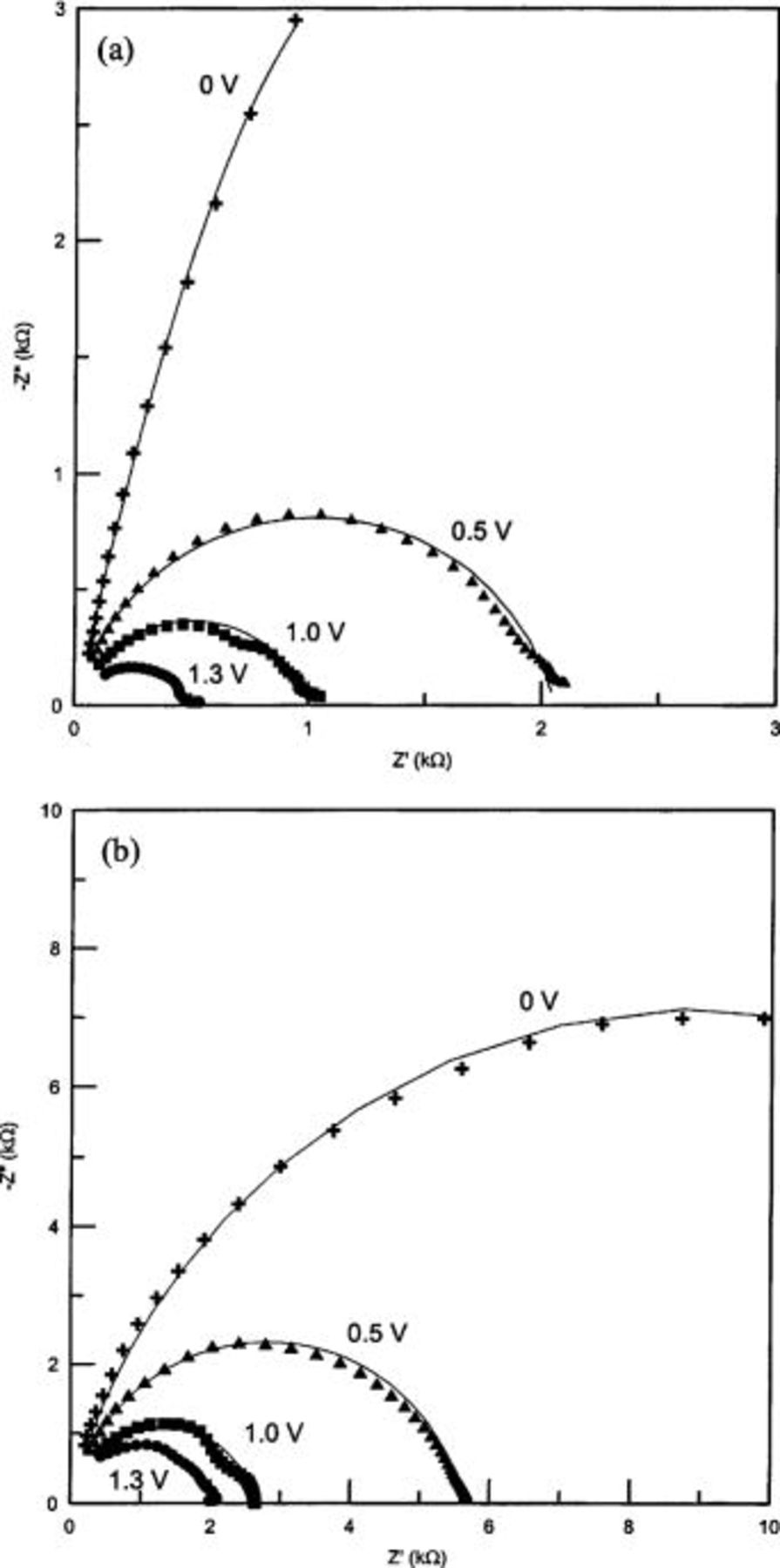
Figure 6. Nyquist diagrams for (a) Au/PANI-a/Al and (b) Au/PANI-b/Al devices measured at different applied bias potentials at 25°C.
Figure 5 and 6 reveal that the impedance response with temperature/bias voltage is a single semicircle. The response can be represented by an equivalent circuit with one parallel RC circuit  and
and  in series with the contact resistance
  10 as shown in the inset of Fig. 5a. The elements of
  and
and  in this model represent the resistance and the capacitance of the depletion layer. Best-fit curves to the equivalent circuit are represented as solid lines in Fig. 5 and 6. The derived best fit values of the corresponding element parameters are presented in Table II. Two striking differences can be noticed in the impedance parameters of device b in contrast to device a. Device b has higher
  and thickness of the depletion layer in comparison to device a, suggesting a build up of an insulating material along with PANI in the case of device b.
Table II.
| The best fitting values of the equivalent circuit elements from the simulation of impedance data for the two devices at different temperatures. | |||||
|---|---|---|---|---|---|
| Device | Temperature(°C) |
 (Ω)
(Ω) |
 (kΩ)
(kΩ) |
 (nF)
(nF) | Wa (nm) |
| Au/PANI-a/Al(device a) | 5 | 48 | 65 | 1.92 | 392 |
| 25 | 40 | 57 | 2.82 | 267 | |
| 45 | 36 | 42 | 2.47 | 304 | |
| 65 | 28 | 18 | 2.25 | 334 | |
| Au/PANI-b/Al(device b) | 5 | 152 | 12 | 1.51 | 498 |
| 25 | 150 | 18 | 1.49 | 504 | |
| 45 | 148 | 17 | 1.44 | 522 | |
| 65 | 118 | 16 | 1.43 | 526 | |
| a W is calculated from Eq. 4 | |||||
Now, it is important to compare the value of  between the two diodes. At any given temperature, the
  value of device b is around 100 Ω higher than that of device a. This result provides clear evidence for the presence of resistive BQ at the Al/PANI-b interface to increase the resistance of simple PANI by a value of 100 Ω.
However, it is worthwhile noting the different behavior of BQ, a molecular material, in comparison to the previous reports of forming a thin insulating film at the metal/polymer interface in the presence of larger size polymeric dopant, polystyrenesulfonate (PSS).4 In the case of PEDOT doped with PSS, two clear partially overlapping semicircles have been noticed.4 The high frequency, bias voltage independent semicircle was attributed to the formation of a thin insulating layer at the metal/PEDOT interface as a result of interaction between sulfonate groups and aluminum atoms. The device structure was interpreted as a metal-insulator-semiconductor junction. The low frequency, bias voltage dependent semicircle has been assigned to the occurrence of a depletion layer. In the present study, a single semicircular impedance behavior was noticed (Fig. 5 and 6) for the metal/PANI-b interface, even in the definite presence of BQ. Hence, the presence of BQ is expected to increase the resistance at the junction by its mere presence at the interface blocking the electrode surface to be in contact with the semiconducting polymer. The reason for the absence of double semicircles in the present study could be determined by exploring more about the parameters related to the depletion layer.
A decreasing trend in the resistance of the depletion region  with the increase in temperature can be seen from the impedance spectra (Fig. 5). The values of
  derived from simulation can be used to calculate the depletion width (W) according to Eq. 4
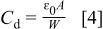
where  is the permittivity of free space and ɛ (assumed to have a value of 3)10 is the relative permittivity of the polymer. The depletion layer for device b is thicker (∼500 nm) than device a (∼300 nm) (Table II). This can suppress the probability of charge transport through tunneling for device b.7 The observed higher
  for device b is consistent with this observation. Otherwise, device a has a thinner depletion width than device b, which arises from the fact that the depletion width is inversely proportional to the conductivity. The increased thickness of the depletion layer can arise from the following reason. When PANI is hydrolyzed to result in BQ, shorter chains of PANI in its reduced form could be formed.17 The coexistence of BQ and reduced PANI with a shorter chain length, makes the matrix more resistive and causes the increased depletion layer. The clear absence of double semicircles in the impedance measurements of our studies is manifested from the comparatively greater thickness of the depletion layer.
Figure 6 shows the impedance characteristics recorded at several applied bias potentials. The values of related parameters obtained from simulation of the equivalent circuit (Fig. 5a) are listed in Table III. The impedance responses (Fig. 6) of both devices strongly depend on the applied bias voltages. In both cases, doping of PANI at higher potentials could be a cause for the decrease in 
Table III.
| The best fitting values of the equivalent circuit elements from the simulation of impedance data for two devices at different applied bias potentials. | |||||
|---|---|---|---|---|---|
| Device | Applied potentials(V) |
 (Ω)
(Ω) |
 (kΩ)
(kΩ) |
 (nF)
(nF) | W a (nm) |
| Au/PANI-a/Al(device a) | 0 | 40 | 57 | 2.82 | 267 |
| 0.5 | 53 | 2.1 | 2.89 | 260 | |
| 1.0 | 55 | 1.1 | 3.51 | 215 | |
| 1.3 | 50 | 0.5 | 3.83 | 198 | |
| Au/PANI-b/Al(device b) | 0 | 150 | 18 | 1.49 | 504 |
| 0.5 | 131 | 5.6 | 1.44 | 522 | |
| 1.0 | 169 | 2.6 | 1.39 | 541 | |
| 1.3 | 126 | 2 | 1.39 | 541 | |
| a W is calculated from Eq. 4 | |||||
Conclusions
The in situ generated hydrolysis products in PANI have significantly increased the contact resistance, barrier height, and width of the depletion layer of the device Au/PANI/Al. As a result, the device fabricated with PANI containing builtin hydrolysis products, shows the different temperature dependence on  characteristics and impedance behavior. The single semicircle impedance behavior in the presence of BQ/HQ at the Al/PANI junction shows that interaction of oxygen groups in BQ/HQ does not contribute to result in the formation of a definite insulating layer as noticed earlier with sulfonate groups from polystyrenesulfonate. The observed difference in junction properties of Al/PANI in the presence of BQ/HQ is manifested from the increased resistance arising from the coexistence of BQ/HQ and reduced PANI with shorter chain lengths at the Al/PANI interface.
Acknowledgments
The authors are grateful to the National Science Council in Taiwan for its financial support through NSC 91-2214-E-006-028 and NSC 92-2214-E-006-003.
National Cheng Kung University assisted in meeting the publication costs of this article.