
Abstract
We investigate the use of random networks of single-walled carbon nanotubes for near-infrared photodetection. By increasing the number of nanotubes between asymmetrical work-function electrodes using dielectrophoretic assembly, the effect of Fermi-level pinning of nanotube-Schottky contacts was revealed in the linear current-voltage characteristic. The extracted device resistance showed an abrupt drop when the numerous intertube junctions formed densely packed networks in the electrode channel. Under the excitation of a near-infrared laser, we performed the photocurrent measurement at ambient temperature at different light powers. Our devices with densely packed nanotube networks showed enhanced photoconductive detection of responsivity, detectivity, and detection response. This is attributed to the increase in the photoabsorption area, the decrease of the channel resistance, and the formation of continuous conducting paths for high-efficient charge percolation. The photoconductive responsivity of up to 8.0 μA W−1 was found with a detectivity of about 4.9 × 105 cm Hz1/2 W−1, which is 4 orders of magnitude greater than that achieved in the channel with individual nanotubes deposited and comparable to that of suspended nanotube bolometers. The densely packed nanotube devices had a detection response of ∼ 4 ms under a finite bias that can be explained by the short-diffusion length of the photoexcited electrons and holes. However, the decrease in the photocurrent with time observed in our devices that exhibited photovoltaic characteristics indicates that electron-hole pair recombination in the nanotube networks occurs with differing characteristic time scales of the injected electrons and holes.
Export citation and abstract BibTeX RIS

Original content from this work may be used under the terms of the Creative Commons Attribution 4.0 licence. Any further distribution of this work must maintain attribution to the author(s) and the title of the work, journal citation and DOI.
1. Introduction
Single-walled carbon nanotubes (SWCNTs) have shown many outstanding electrical properties and a broad-wavelength absorption spectrum for the development of future optoelectronic devices [1–4] including high-performance field-effect transistors [5, 6], gas sensors [7, 8], and biosensors [9, 10]. Most techniques realized so far have exploited semiconducting SWCNTs (s-SWCNTs) or multi-walled carbon nanotubes (MWCNTs) assembled between lithographically patterned microelectrodes on a silicon substrate. The formation of nanotubes in the device channels can be tuned from individually well-aligned to randomly-oriented arrangements with top-down and bottom-up approaches of nanofabrication processes. The commonly used top-down approach is to create a simple SWCNT-field-effect transistor (SWCNT-FET) using symmetrical work-function metal electrodes [11–13]. However, the techniques are limited to batch-to-batch fabrication, and some of them are not compatible with soft substrates due to the requirement of high-temperature grown SWCNTs. On the other hand, the self or directed assembly of nanotubes suspended in aqueous solution offers the possibility of nanoscale-device manipulations with low cost and ease of fabrication [14, 15]. Thus, the quality of the devices fabricated by the solution-processed technique is subject to the purity of the nanotubes and the mixtures of semiconducting and metallic properties [16]. Furthermore, the technique can be deployed on a variety of substrates with the capability to control the number of nanotubes on a large-scale manipulation, enabling more complex circuits to be realized.
Despite its ease of fabrication, one of the main obstacles of the bottom-up approach in the solution-processed technique is to align a large number of nanowires, nanorods, or nanotubes for assembling high-efficiency photodetectors. In particular, when the channel length ( ) of the device is greater than material length (
 ) [17], random networks of the materials tend to form between source and drain electrodes. As a consequence, the electronic properties of the device depend not only on the quality of materials but also on the charge percolation along the channel that is characterized by the percolation density (
 ) [18]. Therefore, the study of percolation transport in random networks could provide an understanding of the device performance in association with charge-carrier mobility, diffusion length, and material density.
In this work, we experimentally characterize the electronic properties of random networks of SWCNT photodetectors implemented using asymmetrical work-function metal contacts by a dielectrophoretic technique. Low and high work-function metals (Al and Au) are used for Schottky and ohmic contacts to the nanotubes, respectively. With this technique, the number of nanotubes in the device channel can be varied from a single few nanotube to a densely packed network. We measure the photocurrent of the devices under the excitation of a near-infrared laser (975 nm) and evaluate their responsivity, detectivity, and time response. We also determine the effect of the number of nanotubes on these indicators of performance. The enhanced photocurrent observed in a channel containing high-density continuous nanotube networks is due to the increase in the photoabsorption area and lower channel resistance.
2. Experimental considerations
Our SWCNT photodetector devices are based on a barrier-free bipolar diode (BFBD) structure that exploits asymmetrical metal contacts to the SWCNTs. Low and high work-function metals (Al and Au) were used to contact the nanotubes at opposite sides to form Schottky and ohmic contacts at Al- and Au-nanotubes, respectively, by dielectrophoretic assembly (DEP). As a consequence, the device behaves as a p-i-n photodiode where p and n conduction is achieved in high and low work-function metals, respectively [19–21]. The devices were prepared on a SiO2/Si substrate using high-purity semiconducting SWCNTs at an initial concentration of 10 μg ml−1 in toluene (NanoIntegris Inc., IsoNanotube-S of 99.9% s-SWCNT [22]). The substrate consisted of a 160 nm thick oxide layer thermally grown on a p-doped Si substrate with a thickness of ∼ 500 μm. An array of Al electrodes (4 pairs in each chip, see figure S1(a) (available online at stacks.iop.org/MRX/8/066303/mmedia)) of supplementary material (SM)) was lithographically defined on the substrate by optical alignment followed by metallization and lift-off process. Each of the pre-defined Al-Al electrode pairs possessed a sharp-end separation of 10 μm (figure S1(b)). The center-to-center of each pair was 200 μm apart on a chip of 6 mm by 6 mm. The Al electrode (60 nm thick) was thermally deposited on the Ti/TiN (20/20 nm thick) adhesion layers. We used an Al electrode (low work-function metal,  eV [23]) with the SWCNTs (
 eV [24]) to create a Schottky barrier for holes at the Al-nanotube contact [25]. For the formation of an ohmic contact to the nanotubes, a high work-function metal, namely, Au (
 eV [23]) was lithographically aligned on top of one end of each Al pair. This was followed by metal deposition of Au (20 nm), as shown in figure S1(c). This Au contact is rectangular (10 μm by 40 μm) to optimize the gradient of the electric field across the device channel [26]. After the lift-off of the Au layer, asymmetrical work-function metal contacts (a Schottky barrier at one end and ohmic contact at the other) were obtained with a channel length reduced to
  μm. The reduced
  is however 3 times larger than the average length of the nanotubes (
 μm) which had a diameter (
 ) of 1.4 nm [22], which could result in random networks of the nanotubes in the device channel. To achieve such asymmetrical metal contacts, one needs one-step lithographical alignment on top of the pre-defined electrode. Next, the surface treatment of the device was performed by a plasma clean under reactive-ion etching (RIE) for the improvement of the contact angle.
The formation of random networks of the nanotubes in the Al-Au electrodes was achieved by applying a droplet containing 3 μl of nanotubes suspended in toluene at the center of the chip with the application of a 1 MHz 10 Vp-p AC voltage using a function generator (Agilent 33210A), as shown in figure 1(a). The oscilloscope (DSO-X 2002A Agilent Technologies) was connected to the DEP circuit for monitoring the assembling signals. In this work, we kept the DEP time to 2 min for each assembling process with four repetitions. Immediately after the application of the AC excitation, the chip was blown dry with nitrogen gas (figure 1(b)). By controlling the nanotube concentration, assembling time, frequency, amplitude of the AC signal, and geometry of the electrodes, we could vary the number of the nanotubes in the device channels of each chip simultaneously. This DEP technique enables the fabrication of SWCNT devices with a simple electronic setup on a stable parametric probing station (this work used the MPS150 module, EPS150COAX DC of Cascade Microtech Inc.), as shown in figures 1(c) and (d). For this study, we fixed the channel length of the electrodes ( μm) and all DEP assembling parameters and varied only the nanotube concentration from 0.01 μg ml−1 to 0.42 μg ml−1.
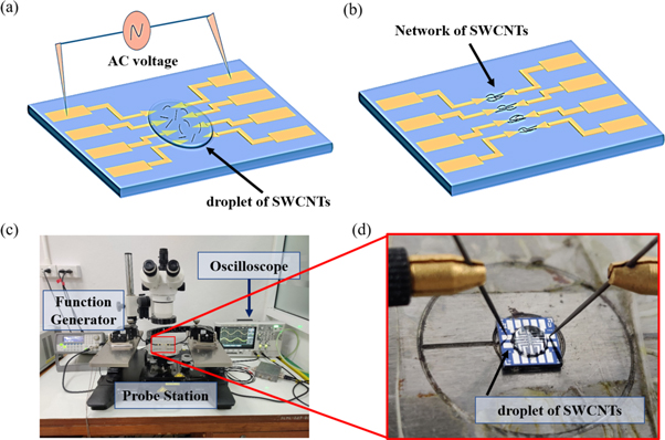
Figure 1. (a) A schematic diagram illustrating the DEP assembly using an AC voltage applied across a pair of electrodes. (b) The random-nanotube networks bridge the electrodes after the application of the AC voltage. (c) A set of instruments required in this work, comprising an oscilloscope, a function generator, and a high-stability electronic probe tester. (d) An actual image of the DEP assembly showing a droplet of SWCNTs and the electrical contacts.
Download figure:
Standard image High-resolution image3. Results and discussion
The variation in the number of nanotubes and the formation of random networks are shown in the scanning electron microscope (SEM) images (figure 2). In figure 2(a), the lowest nanotube concentration (0.01 μg ml−1) was used in the DEP assembly. It shows a small number of intertube junctions in the channel. When the number of nanotubes increased, the distance between two adjacent junctions became shorter and the channel formed densely packed networks with random alignments of the nanotubes (figure 2(d)).
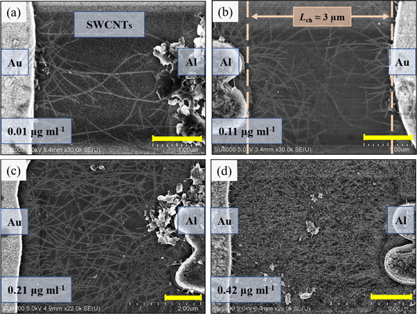
Figure 2. Scanning electron microscope images of the assembled nanotubes by the DEP technique between Al-Au electrodes of channel length  μm for nanotube concentrations of (a) 0.01, (b) 0.11, (c) 0.21, and (d) 0.42 μg ml−1. The scale bar in each image equals 1.0 μm.
Download figure:
Standard image High-resolution imageIn general, the electronic properties of the random-nanotube networks can be determined by the percolation density and the waviness of the nanotubes [17, 18, 27]. Charge percolation through the networks depends on the number of the conducting paths. Charges can percolate from tube to tube if the area density ( ) of the nanotube exceeds the percolation density (
 ), i.e.,
  which gives rise to a continuous film. The device resistance decreased significantly as the number of nanotubes increased. For a fixed channel length (in this work,
  ), the percolation density could be as low as
  μm−2 with the formation of homogeneous nanotube networks expanded in the channel. Random networks of nanocomposite thin-film transistors have been studied to determine charge-carrier mobility (
 ) in long device channels [28–31]. However, these transistors with symmetrical work-function metals for source and drain electrodes could not yield a high sensitivity for photodetection.
In regards to the waviness of the nanotubes in the channel (defined by the curl ratio,  where
where  is the effective length between two ends of the tubes.),
  can determine the electrical properties of the device. The conductivity (
 ) of the channel increases with decreasing waviness, meaning that
  The electrical conductivity of the channel can be described by
  with
with  ranging from 2.2–2.6 in 2D networks and 1.7–2.0 in bulk 3D networks [27, 32]. This suggests that high-efficient charge percolation in random networks or nanocomposites can be achieved in the channel with less waviness of the nanomaterials. For nanotubes that are much shorter than the channel length (
 ), numerous inter-tube junctions have been formed as densely packed networks, suggesting that
  with an expansion across Al-Au electrodes. As a result, the channel can be viewed as a homogeneous film of nanotubes. Our experimental findings confirmed that the increase of the device performance was a result of the increased number of nanotubes in the channel and the lower waviness of them.
To further verify the electronic properties of the random-nanotube networks in the channels, we performed two-terminal DC measurements using Keithley 2450 and 2401 source meter units inside a metal-screened box. Here, the bias voltage was applied to the Au contact by grounding the Al contact. The I-V characteristics of all investigated devices are displayed in figure 3(a). In this work, the devices exhibiting the rectifying behavior with a forward bias ( ) and reverse bias current (
 ) such that
  are obtained for Devices A—C (low nanotube concentrations of 0.01–0.11 μg ml−1). Devices D—F assembled with high nanotube concentrations (> 0.12 μg ml−1) result in linear I-V curves. The data obtained from Devices A, B, and C could be fitted well by the modified diode equation in the thermionic emission model [33],

where  is the reverse-bias current,
  is the diode ideality factor, and
 and
and  are the electric charge, Boltzmann constant, and temperature, respectively. The offset current (
 ) in equation (1) refers to the short-circuit current when the devices are illuminated. The shaded region in high bias (
 V), shown in the inset of figure 3(a) of Device A to C, was fitted to Ohm's law to estimate the channel resistance (
 ) under the forward bias, which approximately equals the series resistance (
 ) obtained in equation (1). Here,
  where
where  is the contact resistance between metal and nanotube, and the sheet resistance,
  where
where 
 and
and  are channel width, film thickness, and film resistivity, respectively. In our two-terminal DC measurement, the value of
  is inaccessible but depends on the metal-nanotube contact area, the intertube junction area, and the barrier height at the metal-nanotube contacts. However, a theoretical study has shown that the contact resistance between nanotubes is approximately 3.4 MΩ [34]. The value of
  could be determined by the physical dimension of the electrode channel and the intrinsic properties of the nanotubes that result in
  Table 1 summarizes
  and
and  that are obtained in the I-V characteristics of figure 3(a) and the estimation using equation (1).
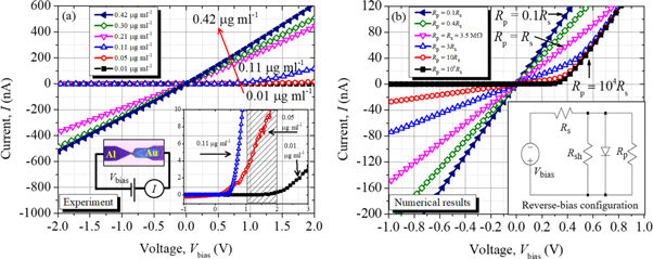
Figure 3. (a) The I-V characteristics of the SWCNT devices fabricated by DEP assembly for various nanotube concentrations. The circuit diagram shows the connection of  across the Al-Au electrode channel. The inset shows rectifying diode characteristics for nanotube concentrations of 0.01, 0.05, and 0.11 μg ml−1 with the shaded area showing the linear I-V regime for the estimation of channel resistance,
  (b) The simulated I-V characteristics of a diode when a variable resistor of
  is connected in parallel to the circuit.
  varies from 0.1
  to 104
 The inset shows the diode equivalent circuit diagram under reverse-bias configuration.
Download figure:
Standard image High-resolution imageTable 1. The extracted parameters using equations (1)–(3) of all investigated devices in this work.
| Device | conc. a (μg ml−1) |

|
 (MΩ) (MΩ) | Detection principle b |
 (V) (V) |

|
 (A W−1) (A W−1) |
 (cm Hz1/2 W−1) (cm Hz1/2 W−1) |
|---|---|---|---|---|---|---|---|---|
| A | 0.01 | 20.1 | 2400 | PV | −0.01 | N/A | N/A | N/A |
| B | 0.05 | 9.5 | 64.7 | PV | −0.01 | 2.6 s | 11.0 × 10⁻¹⁰ | 6.1 × 101 |
| C | 0.11 | 4.3 | 7.2 | PV | −0.01 | 6.6 s | 8.5 × 10⁻¹⁰ | 4.7 × 101 |
| D | 0.21 | N/A | 4.0 | PC | +2.0 | 6.65 ms | 1.4 × 10⁻⁶ | 8.5 × 10⁴ |
| E | 0.30 | N/A | 3.9 | PC | +2.0 | 4.46 ms | 1.3 × 10⁻⁶ | 6.6 × 10⁴ |
| F | 0.42 | N/A | 3.2 | PC | +2.0 | 3.56 ms | 8.0 × 10⁻⁶ | 4.9 × 10⁵ |
a Assembling concentration (conc.). b Photodetection performance under laser illumination (975 nm, 435 mW) showing time response, responsivity, and detectivity of all investigated devices with photovoltaic (PV) and photoconductive (PC) detections.
By further increasing the nanotube concentration from 0.21 to 0.42 μg ml−1 (Devices D—F), the measured current showed a linear dependence of the bias voltage, permitting the estimation of  by Ohm's law suggesting that
  is dominated by
  in the device channel. We see that the experimental results are identical to the numerical simulations when a resistor of
  was connected in parallel to the shunt resistance,
  As shown in figure 3(b) and its inset, the linear I-V curves followed by Ohm's law are obtained by using the LTspice program [35]. When the value of
  is much less than
  we assume that
  is very small. The curves show perfect rectifying diodes when
  is 104
 where
where  is set to 3.5 MΩ. The decrease in
  indicates the increase of the material thickness in a fixed channel length as
  and
and  increase.
We found no significant difference in  as shown 0.16 and 0.26 cm2 V−1 s−1 in Device B (0.05 μg ml−1) and Device F (0.42 μg ml−1), respectively (see data and the calculation in section S2 of SM). Thus, the increase of the electrical conducting in the random-nanotube networks could be verified by the number of nanotubes in the channel, in contrast to the carrier mobility. The appearance of the rectifying behavior in such an asymmetrical Schottky contact structure of low-nanotube concentrations (0.01–0.11 μg ml−1) shows the existence of interface dipoles at metal-nanotube contacts, resulting in the depinning of the Fermi level at the metal-nanotube contact [36]. This is unlikely to happen in a bulk nanotube-metal contact since its barrier height is fixed by the neutrality level of the interface state (
 ). As a result, the Fermi level is said to be pinned inside the nanotubes. Therefore, the choice of low and high work-function metals has not affected the creation of asymmetrical barrier heights for charge injections in the densely packed networks of the nanotubes. This effect can be seen in most metal-semiconductor junctions with bulk-contact structures [37–39]. Furthermore, as the number of nanotubes increases in the random networks, the depletion width (
 where
where  is the dielectric constant of the nanotube and
  is the barrier height) can be reduced by increasing the number of dopants (
 ) for a given
  [40, 41]. Therefore, the lower the
  the more charge injections at the nanotube-metal contacts. As a consequence, the tunneling current dominates the thermionic emission current of a diode in the densely packed networks, resulting in the I-V characteristics following Ohm's law.
We analyzed the electronic properties of the random nanotubes in the channel by plotting  of all investigated devices as a function of the nanotube concentrations. As shown in figure 4 (bottom-left axis),
  decreases rapidly as the concentration increases and remains constant at ∼ 3.5 MΩ for the highest concentration (0.42 μg ml−1). The decrease of
  in the densely packed networks indicates the formation of bulk nanotube-metal contacts as shown by two solid lines, which is confirmed by the increase of current (in the top-right axis at a fixed bias of +1.5 V). The slope of the lines gives the critical concentration of
  μg ml−1.
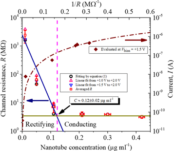
Figure 4. A semi-log plot of  versus nanotube concentration (bottom-left axis) indicates a crossing point between the rectifying and conducting behavior obtained at a critical concentration of
  μg ml−1 at the value of the channel resistance
  MΩ. The measured current evaluated at
  V is plotted as a function of
  (top-right axis) showing the increase of the current with the increase in nanotube concentrations.
Download figure:
Standard image High-resolution imageTo demonstrate the photodetection characteristics, a near-infrared (NIR) laser with a wavelength of 975 nm was used to excite charge carriers in the nanotubes. According to the absorption spectrum of the ultraviolet-visible (UV-VIS) spectroscopy (figure S3) and the material's datasheet [22], the absorption peak was centered at a wavelength of ̃ 940 nm with a broad spectrum of ±100 nm. Thus, the use of light with wavelengths below 840 nm and above 1040 nm is considered as the cut-off wavelength for the NIR photodetection in this experiment. Therefore, our photoexcitation of the wavelength 975 nm of the laser is near the highest photo absorption with the calculated photon energy ( ) of ̃ 1.27 eV which is higher than the energy gap (
 ) of the SWCNTs given by
  eV [42], where the nanotube diameter (
 ) is 1.4 nm. As a result, the excitation by 975 nm laser leads to high-efficient carrier generation in this experiment.
Under the NIR illumination, we demonstrated the photodetection capability of the random-nanotube networks in the DEP assembled devices. We found the photocurrent increased with the number of nanotubes in the channel. The measurement of the photocurrent gives the device photoresponsivity ( ) and detectivity (
 ), which represent the photodetection performance of a photodetector via:


where  is the photocurrent defined by the offset of the measured current of different light conditions,
  and the noise equivalent power
  where
where  is the current noise spectral density. At zero-bias voltage,
  is the measured current given by equation (1) with
  and
and  under the illumination of light (laser 'ON' condition), whilst
  refers to
  when the device was measured in the 'dark' (laser 'OFF' condition).
  is the incident power on the active area (
 ) of the device including the contact pads (see calculation in section S4 of SM).
In figure 5(a), the I-V characteristics of Device B assembled with a nanotube concentration of 0.05 μg ml−1 were taken under the excitation of the NIR laser. The data plotted in the logarithmic scale shows the measured current at two different light conditions. The results indicate a clear difference in the measured current from nearly zero to −2 V, leading to the photocurrent  nA. This detection principle exhibits the photovoltaic (PV) detection characteristic with an open-circuit voltage (
 ) obtained at ∼ +20 mV. The solid lines are fitted by using equation (1). The inset is their linear-scale plots that show a negative
  at
at  in correspondence to the data in the main graph. In figure 5(b), the linear I-V curves of Device F assembled using a nanotube concentration of 0.42 μg ml−1 show the change in the device resistance. The photocurrent of this device was
  nA with the photoconductive (PC) detection under the bias voltage of +2 V which was two orders of magnitude higher than that of Device B.
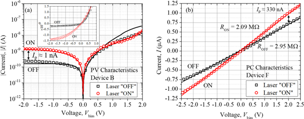
Figure 5. (a) A logarithmic plot of the I-V characteristics of our SWCNT photodetectors during PV detection (Device B) with laser 'ON' and 'OFF' (975 nm, 435 mW). The solid lines indicate the fitting with equation (1). The inset shows the I-V curve in the linear scale (×10–9 A). (b) The photodetection of PC characteristics obtained in Device F with the solid lines for the indications of the resistance change at high absorption.
Download figure:
Standard image High-resolution image
 and
and  as given by equations (2) and (3) are used to assess the detection performance. For all devices measured here, the values of
  and
and  of the devices were found in the range 10–10 to 10–6 A W−1 and 101 to 105 cm Hz1/2 W−1, respectively, after normalizing with the photoabsorption area
  (see the discussion of
  and
and  in the following sections). As summarized in table 1, the data show that
  and
and  are inversely proportional to the channel resistance. In Device A, the photocurrent was impossible to achieve in our measurement setup, due to insufficient light absorption and the high device impedance. The results shown in figures 5(a) and (b) suggest that a considerable increase in
  and
and  could be obtained by further decreasing the channel resistance, which depends on the intrinsic properties of the nanotubes.
The temporal response of the devices was measured via a load resistor of  kΩ to convert the photocurrent into a photovoltage signal displayed by an oscilloscope (input impedance of 1 MΩ and 11 pF). The excitation voltage with a frequency of 1.4 Hz from the wave generator of the oscilloscope was used to modulate the radiation of the laser. Thus, the signal in the voltage response could be converted to the current response after dividing by
  For the estimation of the time response (
 ), the rising signal was estimated between 10% and 90% of the amplitude in a period of the laser modulation.
As shown in figure 6(a),  from Device B shows a small increase at a bias of −0.01 V. This device yielded a
  of 2.6 s, obtained at a laser power of 435 mW. In Device D, E, and F, we found the reduction of the time response of the devices assembled with the nanotube concentrations of 0.42 μg ml−1 (Device F), as shown in figure 6(b). The graph shows that
  ms in Device F, which is less than that reported by some uncooled-bolometer devices using nanocomposite materials [43–45].
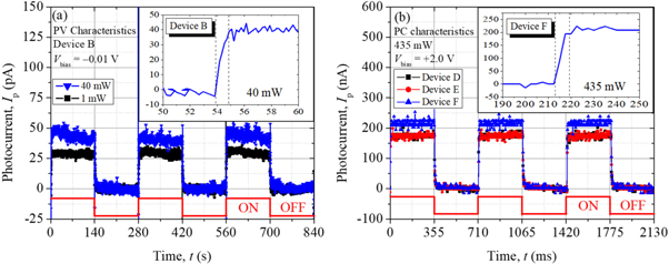
Figure 6. (a) The temporal response of the device assembled with a nanotube concentration of 0.05 μg ml−1 (Device B) under a small bias  V with different laser powers (1 mW and 40 mW) are shown. The inset illustrates the region used for the estimation of the rising time between the dashed lines. (b) The temporal responses of Device D, E, and F (0.21, 0.30, and 0.42 μg ml−1, respectively). The estimated time response of Device F when the signal amplitude is between 10% and 90% is illustrated in the inset under a finite bias (
 V) at the optical power of 435 mW.
Download figure:
Standard image High-resolution imageThe decrease in the photocurrent observed in Device B can be discussed in the context of the electrons (e−) and hole (h+) pair recombination. As shown in figure 6(a), the device has little nanotube deposition in the electrode channel. After photoabsorption in the SWCNTs, e−-h+ pairs are generated in the entire nanotubes. The e− and h+ are separated by a built-in electric field in the depletion region at the Al-nanotube contact where h+ is injected into the nanotubes, resulting in the photocurrent with a PV characteristic at zero-bias voltage. The recombination of e− and h+ takes place outside the depletion region but in the SWCNT networks. As we applied a small bias of  V, the injected h+ from the Al-nanotube contact recombines with the injected e− through the diffusion process in the SWCNTs because of this bias. If
  characterizes the time-dependent number of photogenerated h+ swept into the nanotubes by the built-in electric field and
  defines the number of injected e− by the small bias via the diffusion process, the net charge carriers injected into the nanotubes will suppress the number of holes by the injected electrons from the small bias. The photocurrent of the nanotubes is described by
  where
where  and
and  characterize the time response of the h+ and e−, respectively. Therefore, the photocurrent of the device is a competition between the injected h+ and e−. Furthermore, as there are few nanotubes present in the device channel, e− cannot percolate through the random networks efficiently, leading to a slow time response in comparison to the fast-injected h+ assisted by the built-in electric field at the Al-nanotube junction. Since the depletion width of the junction is much smaller than the channel length and h+ is injected into the nanotubes by the built-in field, this results in
  Thus, the photocurrent observed in Device B with a PV characteristic decreased with time in a favor of the injected electrons through the diffusion process under a small bias. A similar effect has also been observed in graphene/silicon photodetectors [46].
The decrease in the photocurrent with time, however, is not observed in Devices D—F that are operated with a PC characteristic under a large bias voltage (+2 V). These devices possess a large number of nanotube depositions between electrodes with bulk nanotube-metal contacts, resulting in no depletion region and hence no built-in electric field. In these devices, e−-h+ pairs are created by photoexcitation of the photons with an energy higher than the SWCNT energy gap. After the photoexcitation, e−-h+ pairs are separated by an external electric field (e.g.,  V), where the e− and h+ are injected into the metal and nanotubes, respectively. At zero-bias voltage, the net current is zero due to the suppression of the photocurrent by e− and h+ generation in the channel. Thus, the photocurrent in these devices requires a potential difference across the device channel. There is no decrease in the photocurrent with time in figure 6(b) as charge recombination and generation processes are equilibrated under a finite bias.
In the discussion of the time response of the device, a small τ obtained in densely packed nanotubes is attributed to the transit response ( ) of the carriers traveling across adjacent metal electrodes, the diffusion time (
 ) of the excess carriers, and the time constant (
 ) set by the instruments, expressed as
  [47, 48]. In our measurement,
  and
and  were neglected in comparison to
  since these showed nanosecond timescales. The main contribution of
  in our densely-packed devices is described by the diffusion length (
 ) as
) as  [33]. We calculated
  from the measured
  to be ~1 mm and ~48 μm of Device B and F, respectively, by using
  summarized in table 1. The larger
  obtained in Device B implies a large carrier lifetime between photogeneration and recombination of charges, which is desired in photovoltaic-operation devices with no bias voltage. However, a short diffusion time is achieved in densely packed networks (Device F) since the increased number of nanotubes populates the scattering center for charge carriers that result in the reduction of

Figure 7. (a) The current noise spectral density measured by the spectrum analyzer of Device B and F at biases of −0.01 V (red circles) and +2 V (blue triangles), respectively. The noise of the instruments ( ) is shown as black squares when the input of the preamplifier (Signal Recovery 5186 of gain 1000) is shorted by a 50 Ω resistor. The solid line shows the thermal noise (
 ) of
) of  The inset shows the
  of Device F before subtracting
  and
and  measured at a bandwidth of 60 kHz to 99 kHz at different light conditions. (b) The histogram of measured
  in Device F corresponding to the data of the inset of figures 7(a). (c) The circuit diagram of the noise measurement using a bias resistor (
 MΩ) and
  in series with the device (
 ).
).
Download figure:
Standard image High-resolution image
The  of our assembled SWCNT photodetectors was determined using equation (3) with the
  obtained by measuring the voltage noise spectral density (
 ) on
) on  in a specific frequency bandwidth (
 ). In the noise measurement setup, we used
  kΩ. Figure 7(a) shows the current noise spectral density (
 ) of Device B, Device F, the instrument noise (
 A2 Hz−1), and the thermal noise of
  (
( A2 Hz-1) in the frequency range of 10 kHz to 100 kHz. Here we consider our photodetectors as an electrical noise source under the influence of the external bias. For
  kHz, the
  noise of the devices was observed. The cut-off frequency was calculated as
  MHz with
  pF (the capacitance per meter of RG-58 BNC cables and the input of the preamplifier ∼ 20 pF).
In the inset of figure 7(a), the  of Device F was measured at frequencies between 60 kHz and 99 kHz at two different light conditions. The two spectra show a small difference in the noise amplitude in comparison to laser 'ON' and 'OFF', which correspond to the histogram plots in figure 7(b). The data were taken below
  MHz acquired at 751 points after root-mean-square (RMS) averaging of 100 times by the spectrum analyzer (SPA; Siglent 3021x). The resolution bandwidth (RBW) was set to 10 Hz. The bias resistance (
 MΩ) was used to limit the current fed to the device (see the circuit diagram in figure 7(c)).
The histogram plot of Device F at laser "OFF" condition yields the peak at  A2 Hz−1 that can be used to obtain the
  of the device. Thus, by subtracting
  and
and  the actual value of
  is ∼ 4.55 × 10⁻²⁴ A2 Hz−1, resulting in the current noise of
  pA Hz−1/2 generated from Device F. This noise level is much lower than the measured photocurrent (
 nA, see figure 5(b)). Therefore, the
  of Device F was found to be 2.67 × 10⁻⁷ W Hz−1/2. After normalizing with
  the maximum
  was shown to be up to ~4.90 × 105 cm Hz1/2 W−1, obtained in Device F with the densely packed networks (table 1). This value is comparable to some of the bolometers using suspended nanotube films [49, 50]. However, the devices studied here were pristine SWCNTs and so their detection performance can be further improved by incorporating other materials such as graphene, P3HT, polycarbonate, and fullerene (C60), etc., making nanocomposite networks for high-performance photodetectors [2, 51–53].
Our experimental results showed 
 and
and  values of up to 8.0 μA W−1, 4.9 × 105 cm Hz1/2 W−1, and 4 ms, respectively, in the densely packed nanotube networks. This device had a higher gain than the device with a few nanotube depositions (
 and
and  = 1.1 nA W−1, 6.1 × 101 cm Hz1/2 W−1, and 2.6 s, respectively). These values are compared with the other SWCNT photodetectors, assembled with different techniques (table 2).
Table 2. A comparison of the detection performance in carbon nanotube-based photodetectors.
| Nanotube Devices [REF.] | Contact Structure c | Detection Characteristics d | Light Intensity [W cm−2] (Wavelength [nm]) |

| Responsivity | Detectivity [cm Hz1/2 W−1] |
|---|---|---|---|---|---|---|
| SWCNT networks [This work] e | BFBD (Asm) | PV | 2.4 (975) | 2.6 s | 1.1 nA W−1 | 6.1 × 101 |
| SWCNT networks [This work] f | BFBD (Asm) | PC | 2.4 (975) | 3.6 ms | 8.0 μA W−1 | 4.9 × 10⁵ |
| Individual SWCNT [54] | Sym | PV | 7.1 (1550) | 4 ms | 0.18 A W−1 | N/A |
| Well-aligned SWCNTs [55] | BFBD (Asm) | PV | 1570 (785) | N/A | 98 μA W−1 | 1 × 10⁷ |
| SWCNTs/PC71BM [43] | BHJ (Asm) | PV | 0.1 (1010) | 40 ms | 0.02 A W−1 | 2 × 10¹⁰ |
| SWCNTs/polycarbonate [51] | Sym | PC | 0.7 (1300) | 40 ms | 0.4 μA W−1 | N/A |
| SWCNTs/P3HT [2] | BHJ (Sym) | PC | 1.6 × 10⁻² (1000) | 1.4 ms | 16 mA W−1 | 2.3 × 10⁸ |
| MWCNT/graphene [56] | BHJ (Sym) | PC | 3.0 × 10⁻² (1000) | 1.5 ms | 1000 V W−1 | 1.5 × 10⁷ |
| Suspended SWCNTs [49] | Sym | Bolometer | 3 × 10⁻¹ (1300) | 50 ms | 150 V W−1 | 4.5 × 10⁵ |
| Suspended MWCNTs [50] | Sym | Bolometer | 36 (940) | 60 ms | 110 V W−1 | 4.0 × 10⁶ |
c BFBD: barrier-free bipolar diode, BHJ: bulk heterojunction, Asm: asymmetrical metal electrode, Sym: symmetrical metal electrode. d The detection characteristics with photovoltaic (PV), photoconductive (PC), and bolometric behavior. e The PV detection principle (Device B) with nanotube concentration = 0.05 μg ml−1 at Vbias = −0.01 V. f The PC detection principle (Device F) with nanotube concentration = 0.42 μg ml−1 at Vbias = +2.0 V.
4. Conclusions
In conclusion, we have fabricated semiconducting nanotube (SWCNT) photodetectors using dielectrophoretic assembly with low and high work-function metals and studied the electronic properties of the random networks of the SWCNTs under the illumination of a near-infrared (NIR) laser. Our experimental results revealed the effect of Fermi-level pinning of bulk nanotube-metal contacts in the densely packed nanotube networks. After photoabsorption of the NIR laser, the devices showed photovoltaic (PV) and photoconductive (PC) characteristics. The detection performance of the devices determined by photoresponsivity, detectivity, and time response, strongly depends on photoabsorption area, channel resistance, and charge percolation in the random-nanotube networks. The device with densely pack nanotubes showed a photoresponsivity and detectivity of up to 4 orders of magnitude higher than that achieved in the device with a few nanotube depositions. The fast time response in the densely packed nanotube networks under a finite bias is attributed to the short-diffusion length of the photoexcited electrons and holes. The slow injection of electrons via diffusion results in the decrease of the photocurrent in the PV device with the low nanotube deposition. Our experimental investigations on the random networks of the nanotubes suggest a further study using  noise measurement to verify charge percolation in the nanotube networks with different channel geometries.
Acknowledgments
This work was supported by the Thailand Research Fund (TRF) grant no. RSA6080070. Y J acknowledges the Semiconductor Physics Group, Cavendish Laboratory, University of Cambridge, for the clean-room facilities. We are grateful to the Thai Microelectronics Center for the support of microelectrode fabrication. We thank Michael A Allen for proofreading the manuscript.
Data availability statement
All data that support the findings of this study are included within the article (and any supplementary files).