

Abstract
Ab initio calculations on ultra-thin nanofilms of 25 kinds of zinc-blende semiconductors demonstrate their stable geometry structures growth along (1 1 1) surface. Our results show that the (1 1 1) surfaces of 9 kinds of zinc-blende semiconductors can transform into a stable graphitelike structure within a certain thickness. The tensile strain effect on the thickness of graphitic films is not obvious. The band gaps of stable graphitic films can be tuned over a wide range by epitaxial tensile strain, which is important for applications in microelectronic devices, solar cells and light-emitting diodes.
Export citation and abstract BibTeX RIS
1. Introduction
The zinc-blende (ZB) structure is adopted by a wide range of semiconductor materials such as III–V compounds: BN, BP, BAs, AlP, AlAs, AlSb, GaP, GaAs, GaSb, InAs, InP, InSb; II–VI compounds: BeS, BeSe, BeTe; and IIB–VI compounds: CdS, CdSe, CdTe, HgS, HgSe, HgTe, ZnO, ZnS, ZnSe, ZnTe. The ZB lattice structure with sp3-hybridized bonds gives these materials unique physical properties. They have many important applications in the modern microelectronic industry. For example, BN in this form has a variety of interesting properties, including being ultrahard, as well as having a high melting point and high thermal conductivity. So it can be used in cutting and shaping. The films of BN are also of interest, as they are ideal for use as a protective coating on steel. Such films may also be used in the construction of field emitting devices for they have negative electron affinity [1]. BAs of ZB phase is a semiconductor with an indirect electronic band gap measured to be about 1.5 eV and optical properties suggest it may be a good candidate for photovoltaic applications. It has almost purely covalent bonding with the smallest ionicity of all III–V ZB compounds [2]. Moreover, its high lattice thermal conductivity suggests that it is a promising material in thermal management [3]. GaAs, GaSb, InAs and InSb have spin–orbit coupling, which leads to spin relaxation [4], optical spin orientation [5], spin Hall effects [6], persistent spin structures [7], or the spin galvanic phenomena [8]. So they can be used in spintronics devices [9]. Therefore, the research on the properties of their films appear to be very important. BeS, BeSe, BeTe crystallized in ZB phase at ambient conditions have wide band gaps and high bulk moduli. They will transform from the ZB structure to the hexagonal sixfold coordinated NiAs phase at high pressure [10]. CdSe and CdTe thin films are the key components for the next generation of solar cells and other optoelectronic devices [11]. The doping ZnO films are suitable for devices in microelectromechanical and communication systems [12, 13]. V-doped ZnO films can be used as piezoelectric layer in surface acoustic wave devices with high performances [14]. From above, we know that it is necessary to investigate the geometry and the electronic structures of ZB semiconductor materials.
The main goal of this paper is to provide a deeper insight into the geometry structures transition from ZB to graphitic structure for the (1 1 1) surface of ZB semiconductor compounds. This is motivated by the studies on the thin films of wurtzite materials [15–17]. In which,when cleaving the bulk wurtzite (WZ) to obtain the (0 0 0 1) thin films with different layers, there is a surprising transform from wurtzite structure into a stable graphitelike one [16]. In addition, first-principles calculations predict that the thickness range of the stability of graphitic films of WZ materials can be increased by epitaxial tensile strain [15]. Inspired by this series of research, we further investigate the similar nanofilms of ZB structure along (1 1 1) surface and also study the tuning effect of the epitaxial strain on the limit thickness of stable graphitelike structure. Our calculations predict that the epitaxial tensile strain effect on the limit layers of graphitic films is not obvious like that on the WZ materials. Moreover, the band gap of the stable graphitic films can be tuned by the films thickness and strain.
The paper is organized as follows: section 2 describes the calculation method we employed. Section 3 contains the results and discussion. The final section will summarize the main conclusions of this work.
2. Computational methods
Our calculations are performed in the framework of DFT [18] within the generalized gradient approximation (GGA) [19] and the local density approximation (LDA) [20]. The (1 1 1) slabs of the researched ZB materials have been constructed. To ensure a negligible interaction between the slabs, a vacuum gap of 15 Å is added above the surface to simulate the nanofilms. For the exchange-correlation potential [21, 22], the GGA given by Perdew–Wang (PW91) [23] has been utilized. We used ultra-soft Vanderbilt pseudo potentials [24] and an energy cutoff of 480 eV. The reciprocal space integration scheme utilized the Monkhorst-Pack sampling scheme for k points mesh of Brillouin zone with 9 × 9 × 1 is chosen for the surface unit cell. The convergence for total energy is set to be 10−5 eV and all degrees of freedom were relaxed in the geometry optimizations.
3. Results and discussion
3.1. Geometric Structures
25 different ZB structures have been chosen to study in this work, which can be classified into three types, which are III–V semiconductor materials: BN, BP, BAs, AlAs, AlP, AlSb, GaAs, GaP, GaSb, InAs, InP, InSb; II–VI semiconductor materials: BeS, BeSe, BeTe; IIB–VI semiconductor materials: CdS, CdSe, CdTe, HgS, HgSe, HgTe, ZnO, ZnS, ZnSe, ZnTe. We model the nanofilms along (1 1 1) surface based on the above mentioned compounds to investigate their transformation from ZB structures to graphitic structures.
To show that structural changes before and after geometry optimization more clearly, we choose ZnO of ZB structure as an illustration. Figure 1 depicts the structures of ZnO bulk and film. Figure 1(a) shows the unit cell of ZB ZnO bulk, which has two fcc sublattices displaced from each other along the body diagonal by a vector [25]. The nanofilms of ZnO are constructed along (1 1 1) surface. Figures 1(b) and (c) depict the top view of ZnO films with 2 layers and multilayers. It is worth noting that top view of the 2-layer films are different from that of the multilayer films, the former structure is a six-member ring (each ring were consist of 3 cation (Zn) atoms and 3 anion (O) atoms) structure, and the latter has two sets of the six-member ring structure, every two layers for a half cycle of dislocation. For the films optimization, the variation of atom positions are not easily observed after relaxation from top view. Therefore, we give the side view of the nanofilms before and after relaxation in figures 1(d) and (e) for ease of understanding. Much more different from the top view, the side view has great changes by optimization. When the films comprise less than a given number of layers, they are optimized to a graphitic structure thus removing the destabilizing dipole and changing the hybridization from sp3 for ZB structures to sp2 hybridization for graphitic structure [16, 26]. This graphitic structure arises from the atoms within each bilayer converging to just one layer. For ZnO, it makes such a change when the film layers up to 6 layers.
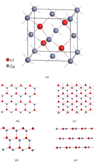
Figure 1. Structure of ZnO bulk and film: (a) the unit cell of ZB ZnO, (b) top view (along z axis) of 2layers films, (c) top view (along z axis) of multilayers films, (d) side view (along y axis) of ZnO films before relaxation, (e) side view (along y axis) of ZnO films after relaxation.
Download figure:
Standard image High-resolution imageIn this work, we study the geometry structures of (1 1 1) nanofilms of III–V compounds: BN, BP, BAs, AlP, AlAs, AlSb, GaP, GaAs, GaSb, InAs, InP, InSb; II–VI compounds: BeS, BeSe, BeTe; And IIB–VI compounds: CdS, CdSe, CdTe, HgS, HgSe, HgTe, ZnO, ZnS, ZnSe, ZnTe. By relaxation, we find that 9 kinds of ZB semiconductors (III–V compounds: BN, BP, BAs, AlP; II–VI compounds: BeS, BeSe; IIB–VI compounds: CdS, ZnO, ZnS) can transform into a stable graphitelike structure within a certain thickness. And this transform is not observed for the other compounds. The maximum number of layers up to which the graphitic structure is stable for the 9 kinds of ZB semiconductors are shown in table 1. We find that BN has the largest transform layer (20 layers). Namely, when BN (1 1 1) nanofilms comprise less than 20 layers, they will become into a flat graphitic structure to reach their most stable geometries. Within 20 layers, BN (1 1 1) nanofilms exhibit semiconductor properties. Beyond 20 layers, they will have metal properties. Similar results are also obtained for BP, BAs, ZnO and BeS as shown in table 1. However, it is worth noting that the results are different for AlP, ZnS, CdS and BeSe, beyond the transform layers, their nanofilms will not immediately transform from semiconductors to metal. For instance, AlP nanofilms are semiconductors with graphitic structure up to 2 layers, and between 4–6 layers they are semiconductors with ZB structure, then they will show metal properties when larger or equal to 8 layers. Similar calculation conclusions can also be drawn for ZnS, CdS and BeSe. That is to say, between the phase of semiconductors with graphitic structure and the metal states, there exists a semiconductors with ZB structure transition state.
Table 1. Maximum number of layers up to which the graphitic structure is stable (without strain and 5% tensile strain) and Minimum number of layers beyond which the films become metal.
| Film | Number of layers (graphitic structure without strain) | Number of layers (graphitic structure 5% tensile strain) | Number of layers (metal) |
|---|---|---|---|
| BN | 20 | — | 22 |
| BP | 4 | — | 6 |
| BAs | 4 | — | 6 |
| ZnO | 6 | — | 8 |
| BeS | 8 | — | 10 |
| AlP | 2 | — | 8 |
| ZnS | 2 | 8 | 10 |
| CdS | 2 | — | 6 |
| BeSe | 4 | 8 | 10 |
According to the research in Wu et al. [15], the tensile epitaxial strain can substantially increase the thickness range of stability of the graphitic nanofilms, and the compressive strain can decrease the range. In this work, we also investigate the strain effect on the (1 1 1) nanofilms of ZB compounds. However, we did not find a significant influence of the 5% tensile epitaxial strain on the thickness range of the graphitic nanofilms for ZB structures. As shown in table 1, only for ZnS and BeSe, the transform range increases to 8 layers under 5% tensile epitaxial strain and for the other nanofilms the number of transform layers have not changed. Therefore, we reach a conclusion that the tensile epitaxial strain effect on the limit layers is not obvious for ZB nanofilms like WZ nanofilms. In addition, we find that the compressive strain can decrease the transform range, which is similar to that of WZ nanofilms [15].
3.2. Electronic structures
In order to further characterize the electronic structures [27] of the graphitic nanofilms [28] and investigate the relationship between the band gap and the layers, we calculated the band structures of all researched compounds. Here we only show ZnO and AlP as examples in figures 2(a.1)–(a.3) and (b.1)–(b.3) respectively. For simplicity, we just give the band structures of the nanofilms with the critical thickness. From figure 2, we can observe that beyond a certain thickness metallization has clearly taken place for all the relaxed nanofilms. Figure 3 shows the band gaps of each compound with the number of layers. For all the researched nanofilms, the general tendency is that the band gap decreases with the increase of the layers. Only for the band gap of BN nanofilms, there is a slight increase at 16 layers and then decrease with the number of layers.

Figure 2. Band structures of different layers of ZnO and AlP. (a.1) ZnO-2layers. (a.2) ZnO-6layers. (a.3) ZnO-8layers. (b.1) AlP-2layers. (b.2) AlP-6layers. (b.3) AlP-8layers.
Download figure:
Standard image High-resolution image
Figure 3. The variation of the band gaps of each compound with the number of layers. The dashed line marks the calculated band gap of the corresponding bulk. (The solid symbols denote the graphiticlike structures and the open hole symbols denote the buckling structures.)
Download figure:
Standard image High-resolution imageBy comprehensive analysis of the electronic and geometric structures, we divided the nanofilms of the researched compounds into two types, namely normal type and abnormal type. The normal type includes BN, BP, BAs, ZnO and BeS, and they have a common characteristic. Namely, the minimum number of layers at which the compounds become metal are two layers more than the maximum number layers at which the structure can become graphitic structure. Here we call these compounds normal type, and figures 2(a.1)–(a.3) shows the band structure of ZnO as a typical example of this type. The abnormal type contains AlP, ZnS, CdS, BeSe, which are different from the normal type. There are transition layers between the semiconductor nanofilms with graphitic structure and the metal nanofilms with ZB structure. And the transition states are semiconductors with ZB structure. We call these compounds abnormal type, and similarly, we present the band structures of AlP as shown in figures 2(b.1)–(b.3) as a typical example of this type. That is to say, the nanofilms of the normal type compounds have two different states and the abnormal type compounds have three different states. When normal type films are semiconductors, they are certainly graphitic structures, and once they become metal, they must be constructed with the ZB structures. However, for the abnormal type films the first state are semiconductors with graphitic structures, just like the normal type. The second state are still semiconductors but with ZB structures (e.g. 4layers and 6layers for AlP as shown in table 1), when the layers are above a certain thickness, they will change into metal with ZB structures. For clarity, we demonstrate the above explaination using table 2 for ease of understanding.
Table 2. Demonstration of the naonfilms of normal and abnormal types. S: semiconductors; M: metal; G: graphiticlike structure; Z: ZB structures.
| Type | Polarity | ||
|---|---|---|---|
| Non-polar films | Polar films | ||
| Normal type (BN, BP, BAs, ZnO and BeS) | S(G) | M(Z) | |
| Abnormal type (AlP, ZnS, CdS, BeSe) | S(G) | S(Z) | M(Z) |
Normally, the nonpolar surface exhibits semiconductor properties and the polar surface exhibits metal properties according to the polarization theory [29, 30], which are consistent with the results of the normal type films. As for the abnormal type films, the semiconductor property of the polar surfaces can be explained as following. By analysis we find that for the nanofilms of AlP, ZnS, CdS, BeSe, their Mulliken charge distribution of the outmost cation and anion changes with the increase of the layers. Taking AlP as an example, the Mulliken charge of the outmost Al and P are 2.32e and 5.58e (4layer), 2.36e and 5.57e (6layer), 2.39e and 5.56e(8layer).... Namely, with the increase of the layers, the dangling-bond band of the cation is filled gradually and then beyond a certain thickness, the metal property appears. However, for the Normal type nanofilms (BN, BP, BAs, ZnO and BeS), beyond a certain thickness, the change of the Mulliken charge distribution of the outmost cation and anion is not obvious, so their conductive property keep constant.
The results of Mulliken charge analyses of (1 1 1) bilayers nanofilms are presented in table 3. The size of the charge transfer from cations to anions is significantly for the nanofilms relative to that of the bulk. The charge variation is different between each nanofilms range from 0.75e (AlP) to 0.22e (BeSe). For the graphitic nanofilms, the charge distribution between cations and anions is much larger than that of the corresponding bulk. It means that the bond between the ions is stronger and the configuration of the film is more stable than that of the bulk. In addition, we also find that the charge transfer is highly restricted to the surface layers and the charge on the atoms in the slab interior is generally close to that in the bulk.
Table 3. Mean Mulliken charges for bulk and the (1 1 1) bilayers (i.e. the two layers are transformed into one).
| Bulk | BN | BP | BAs | AlP | ZnO | ZnS | CdS | BeS | BeSe |
|---|---|---|---|---|---|---|---|---|---|
| Anion | −0.16 | −0.12 | −0.13 | −0.19 | −0.34 | −0.22 | −0.29 | −0.08 | −0.05 |
| Cation | 0.16 | 0.12 | 0.13 | 0.19 | 0.34 | 0.22 | 0.29 | 0.08 | 0.05 |
| Film | BN | BP | BAs | AlP | ZnO | ZnS | CdS | BeS | BeSe |
| Anion | −0.84 | −0.45 | −0.52 | −0.27 | −0.94 | −0.64 | −0.71 | −0.51 | −0.27 |
| Cation | 0.84 | 0.45 | 0.52 | 0.27 | 0.94 | 0.64 | 0.71 | 0.51 | 0.27 |
3.3. Strain tuning effect on the band gaps
Applying mechanical strain [31] on the semiconductor materials to modulate the band gap is a powerful method [32]. So we also explored the influence of strain effect on the band gaps of the nanofilms. We choose 2-layer graphitic nanofilms for each compound under the compressive and the tensile strain range by 10% to investigate the strain tuning effect on the band gaps, and the results are plotted in figure 4.
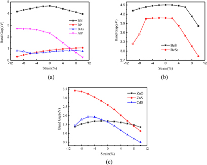
Figure 4. Band gap of 2layers films for each compound as a function of applied epitaxial strain. (a) III–V compound BN, BP, BAs and AlP, (b) II–VI compound BeS and BeSe, (c) IIB–VI compound ZnO, ZnS and CdS. (The solid symbols denote the graphiticlike structures and the open hole symbols denote the ZB structures.)
Download figure:
Standard image High-resolution imageFrom figure 4(a), we observe that for BN, the band gaps decrease no matter their films are under the compressive or the tensile strain. For AlP, the band gaps increase with the increase of the compressive strain and decrease with the the increase of the tensile strain. For BP, the tuning effect is contrary to that of AlP, the band gaps decrease with the increase of the compressive strain and then increase with the the increase of the tensile strain. For BAs, there is a turning point with the strain from compression to tension. In addition, there appear buckling structures with 8% and 10% compressive strain. Figure 4(b) shows that the law of strain regulation for BeS and BeSe, for which we can see that similar to the results of BN, the band gaps of their films decrease with strain. The difference is just that the effect of the tensile strain is more significant than that of compressive strain. From figure 4(b), the sharp decrease of their band gaps happens under the tensile strain. For BeSe [33], there is also buckling exists. Figure 4(c) depicts the band gaps of IIB–VI compound ZnO, ZnS and CdS as a function of the applied epitaxial strain. They have different variation trend. The regulation law of ZnS is similar to that of AlP,and that of ZnO is similar to that of BN. However, for CdS, under the compressive strain, the band gap firstly increases with the increase of the compressive strain and then decreases beyond 6% compressive strain with the buckling geometry transform. Under the tensile strain, the band gap decreases with the increase of the tensile strain.
We choose the buckling structures at 8% compressive strain to demonstrate the structure variation. As shown in figures 5(a) and (b), before applying the compressive strain, the nanofilms are constructed in the graphitic structure and then transform into a buckling structure which is similar to the ZB films. The difference is that under 8% compressive strain, the positions of the cations and anions are exchanged. The bond angle and bond length of BAs, BeSe and CdS before and after applying the compressive strain are listed in table 4. After optimization the angle of the hexatomic ring decreases and the bond length increases. The geometry of the nanofilms changes from sp2 trigonal planar coordination to sp3 tetrahedral hybridization. This is for the reason that this configuration is lower in energy.
Table 4. The bond angle and bond length changes under 8% compressive strain.
| film | Bond angle (°) | Bond length (Å) | ||
|---|---|---|---|---|
| Before | After | Before | After | |
| BAs | 119.867 | 116.845 | 1.791 | 1.819 |
| BeSe | 119.998 | 114.761 | 1.934 | 1.989 |
| CdS | 119.937 | 110.467 | 2.269 | 2.391 |

Figure 5. Buckling structure illustration of relaxed 2layers films (BAs, BeSe, CdS) when applied 8% compressive strain. (a) Before optimization. (b) After optimization.
Download figure:
Standard image High-resolution image
4. Conclusion
In this paper, we investigated the (1 1 1) nanofilms of 25 kinds of ZB semiconductors using first-principles method. By calculation, we find that there are 9 kinds of compounds, which (1 1 1) nanofilms can transform into a stable graphitic structure within a certain thickness. In addition, we find that for the nanofilms of AlP, ZnS, CdS, BeSe, there exist three phases with the increase of the thickness. The regulation law of the strain on the band gaps of stable graphic films is also discussed in detail, which is significant for the basic research and the application in industry.
Acknowledgments
We acknowledge the support from the Fundamental Research Funds for the Central Universities (WUT:2017IB013) and the Natural Science Foundation of Hubei Province under the grant No. 2016CFB586.