

Abstract
Herein we report a prediction of a highly kinetic stable layered structure of tellurium (namely, bulk β-Te), which is similar to these layered bulk materials such as graphite, black phosphorus, and gray arsenic. Bulk β-Te turns out to be a semiconductor that has a band gap of 0.325 eV (HSE06: 0.605 eV), based on first-principles calculations. Moreover, the single-layer form of the bulk β-Te, called β-tellurene, is predicted to have a high stability. When the bulk β-Te is thinned to one atomic layer, an indirect semiconductor of band gap is changed to 1.265 eV (HSE06: 1.932 eV) with a very high kinetic stability. Interestingly, an increase of the number of the β-tellurene layers from one to three is accompanied by a shift from an indirect to direct band gap. Furthermore, the effective carrier masses, the optical properties and phonon modes of few-layer β-tellurenes are characterized. Few-layer β-tellurenes strongly absorb the ultraviolet and blue-violet visible lights. The dramatic changes in the electronic structure and excellent photo absorptivities are expected to pave the way for high speed ultrathin transistors, as well as optoelectronic devices working in the UV or blue-green visible regions.
Export citation and abstract BibTeX RIS
1. Introduction
Since 2004, graphene and related two-dimensional (2D) materials have garnered tremendous interest owing to their many unique characteristics and their potential applications in many electric and optoelectronic devices [1]. 2D materials can be generally divided into two categories: chemical compounds including transition metal dichalcogenides (TMDs) such as MoS2 [2] and WS2 [3], and other compounds such as h-BN [4] and GaS/Se [5]. These compounds have attracted enormous attention owing to their unique properties. Another important category is 2D mono-elemental materials composed of elements near the border between metals and nonmetals. Two-dimensional (2D) mono-elemental semiconductors of group-III, -IV and -V elements have garnered tremendous interest owing to their unique electronic, optical, and chemical properties. For instance, the group-III 2D material borophene [6] has been successfully synthesized and shows metallic characteristics that are consistent with predictions of a highly anisotropic property. In group IV, many 2D materials such as graphene [7], silicene [8], germanene [9] and stanene [10] have been reported experimentally. In addition, the group-V 2D materials phosphorene [11], arsenene and antimonene [12] have been assembled and are subjects of both experimental and theoretical interest owing to their high mobility and superior mechanical, electrical, and optical properties. However, there have been a few reports on group-VI 2D materials owing to their strong nonmetallic properties. It is still an open question on whether the 2D monolayer structure can be realized in group-VI, as has been accomplished for groups-III, -IV, and -V.
Bulk tellurium possesses tetragonal [13], monoclinic (named α-Te) [14] and trigonal [15, 16] crystal symmetries; the lattice structures of each of these three symmetries are depicted in figure S1 (stacks.iop.org/MRX/4/095902/mmedia), and table 1 lists the corresponding lattice parameters. Trigonal tellurium is the most stable in ambient environment [17]; it consists of helical chains and is a semiconducting material with a narrow direct band gap of 0.35 eV, and shows highly anisotropic properties along the c-axis [18]. The three atoms in the unit cell are linked by covalent-like bonds to their nearest neighbors along the chain, whereas the adjacent helical chains are held together by van der Waals interactions. Trigonal tellurium exhibits greatly exceptional characteristics in terms of photoconductivity, catalytic activity, piezoelectricity, thermoelectricity, antibacterial activity, and nonlinear optical response [19–23]. Therefore, its use promises enormous advantages in many applications such as self-developing holographic recording devices, radiative cooling devices, gas sensors, field-effect devices, and infrared acousto-optic deflectors [24, 25]. Moreover, the one-dimensional (1D) trigonal telluriums of nanotubes and nanobelts have been synthesized and applied in various fields [22, 26]. Furthermore, hexagonal Te nanoplates of 32 nm thickness have been successfully achieved on flexible mica sheets by means of van der Waals epitaxy [27]. Recently, ultrathin tellurium nanoflakes have been fabricated and applied in nanogenerators of thickness less than 20 nm [28]. In group VI, tellurium shows the highest electrical conductivity as a semiconductor material, approaching metallic values. Combined with the mentioned performance of tellurium, we like to concentrate our interests on tellurium to investigate whether the 2D monolayer structure can be encountered.
Table 1. The bulk lattice parameters of various crystal systems of tellurium, which have been optimized by DFT-PBE calculations.
| Structure | Crystal System | Space Group | Lattice parameters (Å) | β (°) | α and γ (°) | Numbers of atoms in unit cell | ||
|---|---|---|---|---|---|---|---|---|
| a | b | c | ||||||
| Tellurium | Trigonal | 152( ) ) |
4.456 | 4.456 | 5.921 | 90 | 90 | 3 |
| Tetragonal | 139(D4h [17]) | 7.580 | 7.580 | 10.812 | 90 | 90 | 2 | |
| α-Te | Monoclinic | 12(C2h [3]) | 8.468 | 4.742 | 3.960 | 88.1 | 90 | 6 |
| β-Te | Monoclinic | 12(C2h [3]) | 7.515 | 4.150 | 9.586 | 141.6 | 90 | 6 |
Herein, a new β-monoclinic bulk tellurium (bulk β-Te) and β-tellurene are predicted based on first-principles calculations. All samples are highly stable, which is confirmed with a calculation of phonon spectra and cohesive energies. The predicted bulk β-Te has a layered structure in which adjacent layers are held together by weak interlayer forces with significant van der Waals character. The band gaps of the few-layer β-tellurenes shift from an indirect band gap of 1.265 eV to a direct band gap of 0.404 eV with increasing number of layers from one to three. Moreover, the effective masses of the electrons and holes along the Γ–X and Γ–Y directions in few-layer β-tellurenes are shown to depend strongly upon the number of layers. Finally, optical properties predict high absorptions in the ultraviolet and visible regions.
2. Computational method
All calculations were implemented based on first principles [29, 30]. Phonon spectra were calculated by the method of linear response, which is one of the most popular methods of ab initio calculation of lattice dynamics [31]. Local-density approximation (LDA) [32] was employed to treat the exchange-correlation functional. The treatment of Van der Waals corrections for layered structure was employing OBS dispersion correction [33]. For the following calculations of properties, General gradient approximation (GGA) was used with the Perdew–Burke–Ernzerhof (PBE) functional [34] to describe the exchange-correlation potential. To describe the interlayer van der Waals interactions of the bulk β-Te and multilayer β-tellurene, the Grimme dispersion correction [35] was employed to implement the calculations. All structural models were entirely relaxed until the ionic Hellmann–Feynman forces were smaller than 0.001 eV Å−1 and the energy tolerances were less than 5 × 10⁻⁶ eV/atom. The tolerances of ionic displacement and stress were 5 × 10⁻⁴ Å and 0.02 GPa, respectively. A vacuum of 17 Å between these few-layer β-tellurene structures was adopted, using 9 × 12 × 3 Monkhorst–Pack [36] K-points and the plane-wave cutoff energy of 500 eV.
3. Results and discussion
Utilizing density functional theory (DFT), in the present work we predict a monoclinic bulk β-tellurium with space group C2h [3], named bulk β-Te. Similar to graphite [37], black phosphorus [11] and gray arsenic [12], its layered structure is held together by weak interlayer forces with significant van der Waals character. The most important difference of bulk β-Te with trigonal, tetragonal and monoclinic (α-Te) structures is the presences of graphene-like rings in the  of bulk β-Te, which is corresponding to ab plane in figure 1(c). The bulk lattice parameters of various crystal systems of tellurium is presented in table 1. The single-layer form of the bulk β-Te represents a 2D semiconductor material, namely β-tellurene [38, 39]. Similar to arsenene, the surface of monolayer β-tellurene is wrinkling with incised serrate viewing from the side. The lattice parameters are listed in table 2. The conventional cell of the bulk β-Te contain six Te atoms with a = 7.515 Å, b = 4.150 Å as depicted in figures 1(a) and (b). The orthogonal lattice parameters of monolayer β-tellurene is a = 5.428 Å and b = 4.126 Å (figure 1(c)), containing three Te atoms in unit cell (atomic positions of monolayer β-tellurene detailed in supporting information table S1). Monolayer β-tellurene possesses two types of covalent bonds, Lb = 2.975 Å and Sb = 2.702 Å, and the layer thickness is 2.11 Å. These results are consistent with the previous studies [38–40]. To provide further useful data of the bulk β-Te for its future identification, its x-ray diffraction (XRD) pattern are calculated as shown in figure 2. Obviously, the Miller indices (1 0 0, 1 0 1, 0 1 2, 0 2 1, 1 1 −2, 2 0 2, 1 1 −3, 2 1 −1, 0 2 3, 1 2 2, 1 1 − 4) are coincided with those of JCPDS XRD patterns No.85-555. However, other Miller indices of the bulk β-Te differ from the typical tellurium, and which are attributed to the bulk β-Te.

Figure 1. Atomic configurations after sufficient optimization. (a) and (b) Bulk β-Te from different perspectives, the layer direction along direction of axis c; (c) monolayer β-tellurene. The rectangular box denotes the unit cell of β-tellurene containing three Te atoms. The thickness of monolayer is h = 2.11 Å. Lb and Sb mean long covalent bond and short covalent bond, respectively. (d) Five layers β-tellurene structures (2* 2* 1). The interlayer distance of multilayer is vertical distance between two black lines, and d = 3.843 Å is interlayer distance of bilayer β-tellurene. Other interlayer distances of multilayer are listed in table 2.
Download figure:
Standard image High-resolution imageTable 2. Lattice constants a, b and d (interlayer distance) and in-plane covalent bond lengths of few-layer β-tellurene, using the PBE functional with the Grimme dispersion correction
| NL | Lattice parameters (Å) | d (Å) | Lb (Å) | Sb (Å) | Cohesive energy (eV/atom) | |
|---|---|---|---|---|---|---|
| a | b | |||||
| β-Te | 7.515 | 4.150 | — | 3.027 | 2.808 | 2.763 |
| 1 | 5.428 | 4.126 | — | 2.975 | 2.702 | 2.567 |
| 2 | 5.713 | 4.130 | 3.910 | 3.019 | 2.755 | 2.651 |
| 3 | 5.810 | 4.132 | 3.874 | 3.021 | 2.777 | 2.684 |
| 4 | 5.853 | 4.136 | 3.853 | 3.024 | 2.784 | 2.703 |
| 5 | 5.877 | 4.137 | 3.831 | 3.025 | 2.794 | 2.714 |
aNL represents the layer number, Lb represents the length of the long covalent bond, and Sb represents the length of the short covalent bond.

Figure 2. The calculated XRD spectrum of bulk β-Te, comparing to the standard JCPDS XRD No. 85-555.
Download figure:
Standard image High-resolution imageTo determine whether the structures of the bulk β-Te and β-tellurene have perfect stable structure or not, phonon spectra and cohesive energies are characterized. Firstly, cohesive energies were calculated by  and
and  , where
  ,
,  and
and  is the total energies of a single Te atom, bulk β-Te and tellurenes, respectively. The cohesive energy of monolayer β-tellurene using norm-conserving pseudopotential is 2.567 eV/atom (table 2) which is consistent with that of previous studies (2.56 eV/atom) [39, 40]. Moreover, the cohesive energies computed for few-layer increase with increasing number of layer. Especially, the cohesive energy of the bulk β-Te is larger than that of monolayer β-tellurene by 0.196 eV/atom. Therefore, the formation of the bulk β-Te may require a higher temperature than few-layer β-tellurene. This minor alteration should be attributed to the weak interlayer interactions with significant van der Waals character. Therefore, the interlayer interactions of multilayer β-tellurenes with two to five layers by using the Grimme dispersion correction [35] are shown in figure S2. The cohesive energy computed stands for clear evidence that the structure of bulk β-Te and β-tellurene are bonded by relatively strong covalent bonds. To further verify their structure kinetic stability, phonon calculations were carried out using the density functional perturbation theory (DFPT) [41]. The absence of soft modes in the phonon spectrum is a criterion of structural stability [42]. Significantly, no soft phonon modes in phonon dispersion spectra, which indicates that the bulk β-Te and monolayer β-tellurene are kinetically very stable (figure 3).
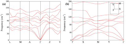
Figure 3. Phonon dispersion spectra of (a) bulk β-Te and (b) monolayer β-tellurene demonstrate highly kinetic stability. The Brillouin zone labeling of the bulk β-Te is placed in table S2.
Download figure:
Standard image High-resolution imageTo examine the electronic properties of the bulk β-Te and few-layer β-tellurene, the band structures and density of states (DOS) were computed as depicted in figures 4 and 5. The results indicated that the bulk β-Te is a semiconductor with an indirect band gap of 0.325 eV (figure 4(a)). Moreover, the calculated total and partial DOS of the bulk β-Te showed that its 5p states are dominant and its 5s states can be ignored near the Fermi level. Contrastingly, away from the Fermi level the predominant contributions to the DOS are those of the 5s states, and the contributions of the 5p states are almost negligible. Importantly, the few-layer β-tellurenes DOSs (figures 4(b) and 5(b)) are coherent and analogous to those of bulk β-Te. Moreover, multilayer β-tellurenes are also semiconductors similar to the bulk β-Te, as shown in figure 5(a). The band gaps decrease with increasing number of layers, which is consistent with the recent experimental result [43, 44]. Moreover, the band structure of monolayer β-tellurene and bulk β-Te were also performed using HSE06 functional [45]. According to the computed results from HSE06 functional, bulk β-Te and monolayer β-tellurene show a large band gap of 0.605 eV and 1.932 eV as illustrated in figures S3(a) and (b), respectively. Significantly, the band gaps of the few-layer β-tellurenes shift from indirect to direct gaps with increasing number of layers from one to three, with the valence band maximum (VBM) and the conduction band minimum (CBM) both located at the Γ point. The band gap can be tuned by increasing layer thickness. Actually, it is well acknowledged that applications of an electric field [46, 47], external strain [12, 48, 49] are all effective ways to adjust the electronic properties of 2D materials. Surprisingly, the band gap of β-tellurene can be regulated by applying external strain [38]. It is therefore expected that β-tellurene has potential use in next-generation electronic and optoelectronic devices.
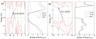
Figure 4. Band structure (left) and partial density of states (PDOS) of (a) bulk β-Te and (b) monolayer β-tellurene with PBE-GGA. The VBM is set to zero energy. Blue arrows denote indirect band gaps.
Download figure:
Standard image High-resolution image
Figure 5. (a) Band structure and (b) partial density of states (PDOS) of multilayer β-tellurenes with PBE-GGA. The blue arrow denotes indirect band gap while red arrow denotes direct band gap. The VBM is set to zero energy.
Download figure:
Standard image High-resolution imageNext, we focus our attention on the effective masses of few-layer β-tellurenes. The effective masses of the electron and the hole were computed as listed in table 3 and shown in figure S4. For monolayer β-tellurene, the computed effective electron masses are  = 0.496 m0 and
  = 0.197 m0, and the effective hole masses are
  = 0.074 m0 and
  = 0.334 m0. The effective mass of the hole is lower than that of the electron along the Γ–X direction. This result indicates that the carrier mobility is governed by holes in monolayer β-tellurene. It should be noticed that the effective carrier masses of monolayer, trilayer and pentalayer β-tellurenes decrease with increasing number of layers along the Γ–X direction. However, for bilayer and tetralayer β-tellurenes, their effective electron masses increase with increasing number of layers along both the Γ–X and Γ–Y directions. The electron and hole masses show a strongly layer-dependent evolution along Γ–X and Γ–Y, respectively. This result presents that electron and hole masses, respectively, decrease from 0.496 m0 and 0.334 m0 for the monolayer to 0.139 m0 and 0.142 m0 for the five-layer system (figure S4).
Table 3. The calculated effective mass of electron and hole in few-layer β-tellurene
| Type | NL |  /m0 /m0 |
 /m0 /m0 |
|---|---|---|---|
| e | 1 | 0.496 | 0.197 |
| 2 | 0.167 | 0.254 | |
| 3 | 0.212 | 0.422 | |
| 4 | 0.169 | 0.338 | |
| 5 | 0.139 | 0.277 | |
| h | 1 | 0.074 | 0.334 |
| 2 | 0.095 | 0.149 | |
| 3 | 0.062 | 0.193 | |
| 4 | 0.078 | 0.189 | |
| 5 | 0.043 | 0.142 |
aTypes 'e' and 'h' denote the 'electron' and 'hole', respectively.  (
( ) (in unit of m0) represents the effective mass along the Γ–X (–Y) direction.
To further investigate the properties of few-layer β-tellurenes, we characterized their optical properties and Raman spectra (figure 6). Raman spectra were calculated by using the laser wavelength of 514.5 nm and the temperature of 300 K. The previous calculated phonon dispersion relation (figure 3(b)) shows that, monolayer β-tellurene totally has 9 phonon modes, 3 of which are Raman-active: 2 Ag modes and 1 Bg mode; 3 of IR-active (Infrared Radiation): 1 Au mode and 2 Bu modes. The calculated frequency values and the corresponding to 9 phonon modes are listed in table S3. The Ag and Bg modes represent different symmetry modes: Ag represents the vibration mode of tellurium atoms along the direction of the layer, whereas Bg represents the vibration mode of tellurium atoms perpendicular to the atomic plane. Table S4 lists the calculated phonon modes of other few-layer β-tellurenes. The characteristic peak Ag mode from high frequency shifts to lower regions with increasing number of β-tellurene layers. This shift is especially prominent between the monolayer and bilayer materials.
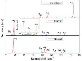
Figure 6. Raman spectra of layered β-tellurene, calculated by means of DFPT. Inset: detailed view of the spectrum for bilayer β-tellurene. The simulation was performed with 514.5 nm laser excitation. Peak frequencies are given in units of cm−1.
Download figure:
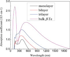
Standard image High-resolution imageIn this section, the optical absorption coefficients of bulk β-Te and of few-layer β-tellurenes were calculated, as presented in figure 7. The absorption intensity of the few-layer β-tellurenes increased with increasing number of layers. Compared to few-layer β-tellurenes, the bulk β-Te exhibited the maximum absorption intensity at the wavelength of 140 nm, which is in the ultraviolet region. For few-layer β-tellurenes, the absorptivity more than 0.5E5 cm−1 starts at the wavelength of 175 nm, and progressively extend to visible region. The peak of absorptivity occurs in blue-violet visible regions. All these results indicate that the new bulk β-Te, few-layer β-Te, and β-tellurenes will be suitable for UV–visible and acousto-optic deflectors due to their optical absorption in the ultraviolet and visible regions.
Figure 7. Calculated optical absorption coefficients of bulk β-Te, few-layer β-tellurenes and β-tellurenes.
Download figure:
Standard image High-resolution image
4. Conclusions
In summary, a new layered structure of the bulk β-tellurium and a 2D mono-elemental semiconductor β-Te material of group VI were predicted by utilizing DFT. High stability of the bulk β-Te, and β-tellurene were proved by calculating phonon spectra and cohesive energy. The cohesive energy of the bulk β-Te is 2.763 eV/atom, which is larger than that of monolayer β-tellurene by 0.196 eV/atom. This result demonstrates that the new architectures possess strongly covalent bonds. Moreover, the calculated Raman spectra present a red-shift with increasing number of layers. The calculation of electronic properties demonstrates that the bulk β-Te has a narrow band gap of 0.325 eV (HSE06: 0.605 eV), but monolayer β-tellurene has a larger band gap of 1.932 eV (HSE06). Significantly, the band gaps of few-layer β-tellurenes shifted from indirect to direct gaps with increasing number of layers from one to three. Moreover, the electron and hole masses of few-layer β-tellurenes show strongly layer-dependent evolutions along the Γ–X and Γ–Y directions, respectively. Optical absorption coefficients show that the bulk β-Te, few-layer β-tellurenes, and β-tellurene are suitable for UV–visible and acousto-optic deflectors due to their absorptions in the ultraviolet and visible regions. It will be very interesting to experimentally realize these indirect–direct band gap semiconductors for nanoelectronic and optoelectronic devices.
Acknowledgement
This work was supported by the National Natural Science Foundation of China (No. 21376199 and 51002128) and IBS-R011-D1.
Author contributions
The manuscript was written through contributions of all authors. All authors have given approval to the final version of the manuscript.