

Abstract
Transparent and highly photoconductive nano-composite ZnO–CdO films were fabricated on glass substrate at 360 °C substrate temperature. X-ray diffraction (XRD) studies indicate that the films are nano-crystalline and contain a combination of hexagonal ZnO and cubic CdO structures. According to scanning electron microscopy (SEM) studies, the surface of the films is found to be rough over large areas favoring photo absorption. From the optical and electrical measurements, it is found that ZnO–CdO composite combines the properties of optical transparency in the visible region with a high electrical conductivity. Based on the characteristics of photoluminescence (PL) and photoconductivity, it seems that Zn/Cd = 3:1 nano-crystalline film is preferable for application as buffer layers in solar cells.
Export citation and abstract BibTeX RIS
1. Introduction
Thin films of n-type transparent conducting oxides (n-TCO's) such as zinc oxide (ZnO) and cadmium oxide (CdO) have received considerable attention mainly due to their enormous potential applications, which include buffer layers for solar cells, photovoltaic solar cells, gas sensors, transparent electrodes and other opto-electronic devices [1–5].
For the development of buffer layers, photoluminescence (PL) and photo response to the electromagnetic spectrum are two highly significant parameters. Luminescence is one of the most used by its application in the development of optoelectronics devices. When light of appropriate energy is incident on a material, photons are absorbed and electronic excitations are created. Eventually, these excitations relax and the electrons return to the ground state. If radiative relaxation occurs, the emitted light can be collected and analyzed to yield a wealth of information about the photo-excited material [6].
Photoconductivity is considered to be an important tool for providing information regarding the nature of the photo-excitations. In the photoconduction mechanism, oxygen molecules are adsorbed at the film surface capturing the free electron present in the n-type semiconductor. These free electrons form a low-conductivity depletion layer near the surface under UV illumination. In this process, photo generated holes migrate to the surface and are trapped, leaving behind unpaired electrons that contribute to the photocurrent. Therefore, a good photoconductive device requires efficient charge separation and efficient transport of charge carriers to electrode [7]. The rise and decay of photocurrent are governed by the trapping states or recombination centers lying in the forbidden energy zone of a photoconductor. Therefore, their variations can be used to understand the nature and distribution of traps and recombination centre [8, 9].
It is well known that, ZnO is a polar inorganic and versatile II–VI semiconductor crystal with hexagonal wurtzite structure that usually has high resistivity with a band-gap around 3.37 eV. The bandgap of pure ZnO can be engineered by cationic Cd2+ substitution, which is an effective tool to tune structural, electrical and optical properties [10]. The free-exciton binding energy of ZnO crystal is 60 meV at room temperature. This is one of the highest values among other optoelectronic materials. This binding energy allows the excitonic transitions to occur even at room temperature, which leads higher radiative recombination efficiency for spontaneous emissions [11]. Another advantage of ZnO is it absorbs larger fractions of solar radiation than other materials [12]. The high thermal energy of ZnO (25 meV) leads to the extreme stability of excitons at RT and high temperatures [13]. CdO is also a II–VI semiconductor with rock salt structure of relatively low resistive and narrow band-gap energy lies between 2.2 eV and 2.5 eV depending upon the growth conditions [14]. This narrow band gap value makes CdO a suitable candidate for combining with ZnO for the fabrication of buffer layers [15]. Therefore, it is expected that the homogeneous composing of these two materials forms a ternary compound that allows intermediate optical and electrical properties between those of pure CdO and ZnO, making it attractive for the fabrication of buffer layers on solar cells. In this work, ZnO–CdO nano-composite thin films are fabricated by a simple and inexpensive chemical spray pyrolysis (CSP) method giving more concentration on studying its PL and photoconductivity properties of different compositions for use as an absorber in solar cells.
2. Experimental
ZnO–CdO thin films were deposited on slide glass substrate at substrate temperature 360 °C using low cost chemical spray pyrolysis (CSP) method [16]. The glass substrates were cleaned by using lukewarm aqueous solution of sodium carbonate, nitric acid and distilled water. The spray solutions were prepared in the following steps: at first, 0.1 M of zinc acetate dehydrate [Zn(COOCH3)2.2H2O] and cadmium acetate dehydrate [Cd(COOCH3)2.2H2O] were prepared separately and diluted in ethanol and de-ionized water at 1:1 ratio. Then to obtain ZnO, CdO and ZnO–CdO thin films, Zn-acetate dehydrate and Cd-acetate dehydrate of 0.1 M were mixed together in different solution ratios. The ratios of Zn/Cd were 1:0, 3:1, 1:1, 1:3 and 0:1. The resulting mixture was stirred at room temperature until a colorless and transparent solution was obtained. The pyrolyzing solution flow rate and gas pressure was kept in the range 1.0 ml min−1 and 105 N m−2, respectively. The spray nozzle to substrate distance was kept at 0.21 m. The spraying time was 20 min and the substrate temperature was kept at 360 °C. The temperature was controlled through a copper-constantan thermocouple. All these growth parameters were kept identical to grow film of almost equal thicknesses. The thicknesses of the films were (180 ± 20) nm measured using Newton's rings method. The crystalline structure of the films was analyzed by means of a SHIMADZU XRD 6000 x-ray diffractometer. The x-ray Cu kα monochromatic radiation of wavelength λ = 0.154187 nm was used to record the diffraction profile in between the Bragg angle of (28–60)°. Surface morphology was studied by using a Hitachi scanning electron microscope (SEM; S-3400N) with accelerating voltage 15 kV. Optical data of the films were taken with a double beam UV-1601 PC Shimadzu visible spectrophotometer. PL measurements were performed at room temperature using a spectrofluorophotometer (RF-5301, Shimadzu, Japan) at an excitation wavelength of 280 nm. The temperature dependent resistivity of films was measured by the usual Van-der-Pauw method of four probe configurations in air ambient using a Keithley electrometer. The photo conductivity of pure ZnO, CdO and ternary ZnO–CdO thin films were measured using an artificial solar simulator AM1.5 (Model: SET-140F, SERIC Ltd Japan).
3. Results and discussion
3.1. Structure and morphology
The x-ray diffraction (XRD) patterns for ternary ZnO–CdO composite nano-material deposited at different Cd volume ratios in solutions are presented. These spectrograms were recorded over 28–60° and are shown in figure 1. The XRD pattern clearly shows the polycrystalline nature of the films. The wurtzite (hexagonal) ZnO and cubic CdO structures have been confirmed by analyzing XRD data of major characteristic peak positions fitting with standard JCPDS card file no. 361451 and 732245. The Miller planes are identified as (1 0 0), (0 0 2), (1 0 1), (1 0 2) for ZnO, and (1 1 1), (2 0 0), (2 2 0) for cubic CdO. For equal volume of Zn/Cd, XRD patterns of ZnO and CdO phases are clearly separated and free of noise. However, for Zn/Cd = 3:1 and 1:3, due to the starting of structural modulation either phase is partially stable and as a result XRD patterns of these samples contain noise compared to other samples. This result indicates that there is interplay between two phases. It seems that when Zn/Cd = 1:1, coexistence of two structures ZnO and CdO (hexagonal and cubic) are thermodynamically more stable and the orientation of crystallization process changes to the direction of minimum energy. This result is supported by intensity data. With the increase of cadmium molar fraction, the intensity of ZnO peaks decreases and the intensity of cubic CdO phase growing in compensation of hexagonal ZnO phase. Such mixed crystallites and phase modulation was reported [17, 18].
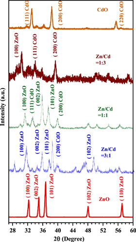
Figure 1. XRD patterns of ZnO–CdO thin films.
Download figure:
Standard image High-resolution imageThe values of (d100) and (d002) planes for ZnO and (d200) for CdO were calculated from the intensity data of the XRD spectra and are tabulated in table 1. It is seen that small differences are observed between d-values of synthesized and standard samples. These small differences may be inherent from chemical, different experimental atmospheres, and from the defects which occur during the deposition. The lattice parameters a and c were calculated using the major peak and the values are a = 0.3240 nm and c = 0.5206 nm for hexagonal ZnO and a = b = c = 0.3346 nm for cubic CdO structure. The average grain size of ZnO–CdO modulated phase was calculated using the Debye–Scherrer's formula. The crystallite size of ZnO (d100) plane decreases from 28 nm to 21 nm, whereas the crystallite size of CdO (d200) increases from 13 nm to 21 nm when Cd ratio increases. This can be attributed to the larger ionic radius of Cd2+ (0.074 nm) than that of Zn2+ (0.065 nm).
Table 1. Standard and observed dhkl values of ZnO–CdO thin films.
| ZnO (dhkl) (nm) | Zn/Cd = 3:1 (dhkl) (nm) | Zn/Cd = 1:1 (dhkl) (nm) | Zn/Cd = 1:3 (dhkl) (nm) | CdO (dhkl) (nm) | ||||||
|---|---|---|---|---|---|---|---|---|---|---|
| Plane | Stnd. | Obs. | Stnd. | Obs. | Stnd. | Obs. | Stnd. | Obs. | Stnd. | Obs. |
| (d100) | 0.2815 | 0.2787 | 0.2815 | 0.2892 | 0.2815 | 0.3025 | 0.2814 | 0.3021 | — | — |
| (d002) | 0.2597 | 0.2567 | 0.2644 | 0.2620 | 0.2644 | 0.2646 | — | — | — | — |
| (d200) | — | — | 0.2347 | 0.1817 | 0.2347 | 0.2328 | 0.2347 | 0.2324 | 0.2340 | 0.2349 |
SEM is a compatible technique to study the surface morphology of thin films. The SEM micrographs of ZnO–CdO composite revealed a close packed morphology. In figure 2(a), complicate polyhedrons shape with a rather compact surface was observed for pure ZnO, this does not show any fissures or disturbances. Fiber- or tissue-like structure was found for Zn/Cd = 3:1 films, as shown in figure 2(b). After that, with increasing the volume of Cd content to the composite, nano-grains were observed to be dense and flake-like with little agglomerations. From the micrographs, it is clearly observed that film surfaces were slightly rough. The roughness is due to the increased optical scattering of incident light on the film surface [19] which may reduce the transmittance of the films. This rough surface morphology of the films is vital for the application as buffer layers of solar cells because it can provide light scattering and subsequently light trapping inside the solar cells structure [20].
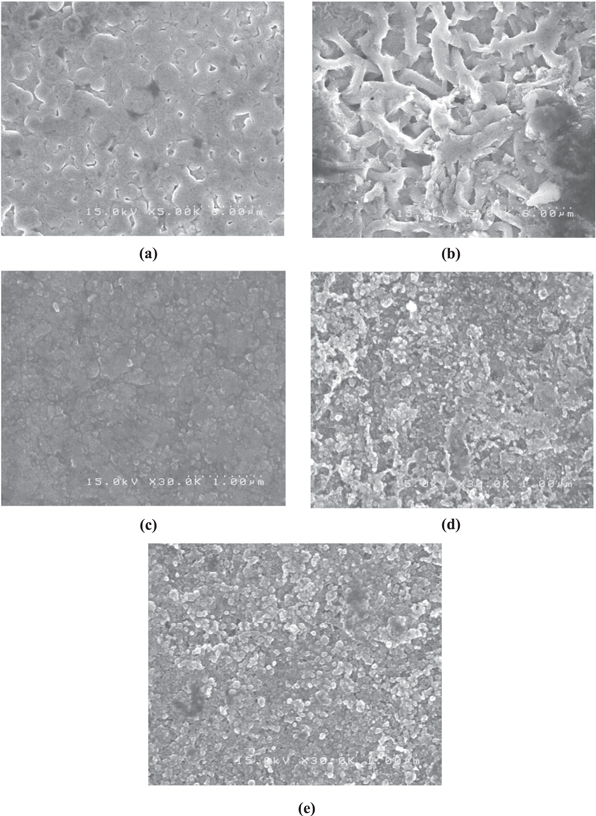
Figure 2. Representative SEM images showing the surface morphology of ZnO–CdO thin films.
Download figure:
Standard image High-resolution image3.2. Optical properties
To analyze the optical properties of ZnO–CdO nano-composite, the transmittance spectra are shown in figure 3. From the graph, it is evident that the transmittance decreases with increasing Cd content and the reflectance is below 8%. This behavior can be attributed due to free electron absorption which confirms the increase of carrier concentration with increasing Cd content that also increases the electrical conductivity of the films. This result agrees very well with surface morphology of the films.
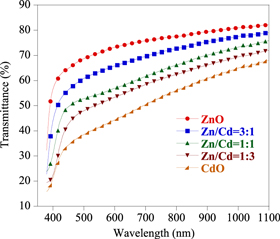
Figure 3. Transmittance spectra of ZnO–CdO thin films.
Download figure:
Standard image High-resolution imageFor the design of optoelectronics device, the band gap modulation is one of the key requirements. The optical band gap  of the system can be obtained by assuming a direct transition between the edges of valance and conduction band. This was calculated from the optical absorption spectra by using Tauc's energy exponential relation [21]

where  is the absorption coefficient,
  is the band gap corresponding to a particular transition occurring in the film,
  is the band edge constant,
  is the transition frequency and the exponent
  characterizes the nature of band transition and assumes the value 1/2 for allowed direct transition. Since ZnO and CdO films are both direct band gap semiconductors, can be calculated by using
  versus photon energy
  plot shown in figure 4. The value of
  decreased from 3.20 eV to 2.21 eV and exhibits a red shift with the rise of Cd concentration from 0 to 1. The observed red shift indicates the presence of native point defects in the ZnO–CdO composite. These native defects are the possible source of n-type carriers which causes the increase of carrier concentrations as well as increase conductivity of the films. The variation of with Cd content is shown in the inset of figure 4. The narrowing band gap is due to the fact that band gap of CdO (bulk value 2.23 eV) is less than that of ZnO (bulk value 3.32 eV) [22]. The decrease in band gap can also be explained with the existence of Cd impurities in the ZnO structure, which induce the formation of new recombination centers with lower emission energy [23]. However, Zhang et al [24] reported that the bottom of the conduction band consists of Zn-4s and O-2p states, and the Zn-4s states are dominant. Incorporation of Cd-5s can enhance s states. With increasing Cd-doping concentrations, the s states at the bottom of the conduction band become stronger hence leading to a conduction band shift and band gap narrowing.

Figure 4. Determination of the optical band gaps from the plots of (αhν)2 versus photon energy.
Download figure:
Standard image High-resolution imagePL is a strong characterization strategy to study the optical emission of thin films. Figure 5 shows the PL spectra of ZnO, CdO and their mixed oxide films under excitation wavelength 280 nm. In the present work, both strong broad peaks and relatively weak peaks were observed at 391 nm for ZnO, Zn/Cd = 3:1 and other films, respectively. The observed peak corresponds to near-band-edge (NBE) with deep level emissions. This UV band was due to the recombination of free excitons through an exciton–exciton collision process. Here, deep level emissions are associated with the single ionized oxygen vacancy in ZnO and results from the recombination of a photo generated hole with the single ionized charge state of the defect [25]. Moreover, all samples exhibit another weak peak at 500 nm which corresponds to green band. This emission is attributed to singly ionized oxygen vacancies and zinc interstitials [26, 27] and comes from the transition from shallow donor levels (interstitial Zn) to shallow acceptor levels (Zn vacancies).
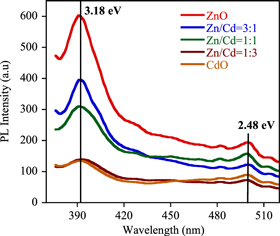
Figure 5. Room temperature photoluminescence spectra of ZnO–CdO films.
Download figure:
Standard image High-resolution image3.3. Electrical properties
The temperature dependent electrical conductivity of ZnO–CdO nano-composite was measured using Vander Pauw's method in air ambient, as shown in figure 6. The activation energies ΔE1 in the temperature range (300–373) K and ΔE2 in the range (374–450) K were obtained from the straight part of the logarithmic conductivity with inverse temperature graph. It is seen that ΔE2 is higher than that of ΔE1, as is given in table 2. The higher values of ΔE2 indicate that the conductivity is associated with the free band transition of carriers. The low values of ΔE1 may be associated with the hopping of localized levels due to the excitation of carriers from one defect state to another. Furthermore, from figure 6 it is seen that the activation energy decreases with the increase of Cd concentrations. This leads to the decrease of band gap suggesting that band gap could be controlled by means of a change in Cd concentration. Also, by adding Cd, the higher crystal orientation can be thought of to enrich the conductivity. This can be explained due to the increase of charge carrier mobility because the shorter carrier path length in a c-plane and the reduction in the scattering of the charge carriers of the crystal defects [28].

Figure 6. Determination of activation energy at two different temperature regions (a) 303–373 K and (b) 374–450 K for ZnO–CdO thin films.
Download figure:
Standard image High-resolution imageTable 2.
Crystallite size (ζ), band gap energy (), activation energy(ΔE) and RT resistivity of ZnO–CdO thin films.
| Activation energy ΔE (eV) | ||||||
|---|---|---|---|---|---|---|
| Sample | Crystallite size of ZnO (100) ζ (nm) | Crystallite size of CdO (200) ζ (nm) | Band gap (eV) |
ΔE1 (303–373)K | ΔE2 (373–448)K | RT resistivity (ohm-cm) |
| ZnO | 28 | — | 3.20 | 0.11 | 0.36 | 56.1 |
| Zn/Cd = 3:1 | 27 | 13 | 2.97 | 0.058 | 0.15 | 14.0 |
| Zn/Cd = 1:1 | 25 | 16 | 2.70 | 0.093 | 0.42 | 4.0 |
| Zn/Cd = 1:3 | 21 | 18 | 2.43 | 0.0085 | 0.23 | 0.8 |
| CdO | — | 21 | 2.21 | −0.0077 | −0.015 | 0.00042 |
Photoconductivity is defined as the net charge in electrical conductivity under illumination. This process involves the absorption of energy from light or from particles, the excitation of charge carriers from a non-conducting ground state to a higher energy state where they are free to contribute to the electric conductivity and the return of charge carriers from the conducting state to ground state. Figure 7 shows the photoconductivity transients of the ZnO–CdO nano-films carried out as a function of a constant light intensity. All measurements of the current were carried out at room temperature and ohmic nature of the contacts was ensured. From I–V measurements, it is observed that for ZnO and Zn/Cd = 3:1 nano films photo current increased 1000 times compared to dark current. However, for other samples photocurrent increased only 10 times. It seems with illumination, electron–hole pairs are generated inside the films by light absorption. As a result, electrons are captured by negatively charged oxygen ions. These oxygen photo-desorption electrons are successively reintroduced into the conduction band. At the same time, the electron–hole pairs are separated by the electric field. Hence the depletion region of the films destroys and generates to an increase of photoconductivity. So transition from localized states within the forbidden gap is speculated to be the reason for high photo current. It seems when Cd concentration increases the film grain boundary increases simultaneously. Since deposition of the films was carried out in air ambient, chemisorbed oxygen at grain boundaries depletes free electron that reduces the photo current of Zn/Cd = 1:1. 1:3 and CdO films.

Figure 7. Variation of photocurrent and dark current with bias voltage for ZnO–CdO films under artificial sun light.
Download figure:
Standard image High-resolution imageThe time-resolved rise and decay of photocurrent spectra for ZnO–CdO nanoparticles under visible illumination with fixed photo-flux and bias voltage is shown in figure 8. For ZnO, Zn/Cd = 3:1 and Zn/Cd = 1:1 nano films photocurrent increases while dark current decreases with time. But for Zn/Cd = 1:3 and CdO films time-resolved rise and decay exhibits an anomalous behavior of photo-current where dark current also increases with time. This anomalous behavior may be attributed to high rate of re-adsorption of oxygen molecules.

Figure 8. Variation of photocurrent and dark current with time for ZnO–CdO films at constant bias voltage.
Download figure:
Standard image High-resolution imageThe ratio of photoconductivity and dark conductivity is called the photo response. This parameter indicates the suitability of a material for use as a buffer layer in a solar cell device and can be expressed as [29]

where Ilight and Idark are the currents measured under illumination and in the dark, respectively. The photo-response characteristics of the films are shown in figure 9. As seen in figure 9, the Zn/Cd = 3:1 film exhibits about 6 times higher photo-response compared to ZnO film while 100 times greater photo-response than other Zn/Cd films. Therefore, it is clear that this particular Zn/Cd = 3:1 film can capture more electrons on visible illumination and released into conduction band that enhances the photoconductivity of the film.

Figure 9. Time resolved photosensitivity of ZnO–CdO films.
Download figure:
Standard image High-resolution image
4. Conclusions
In summary, we have studied the structural, morphological, optical and photo-electrical properties of ZnO–CdO nano-composite films prepared by a simple and inexpensive CSP technique. The structures of ZnO–CdO nanofilms were characterized by XRD which revealed the formation of polycrystalline films with hexagonal wurtzite ZnO phase and a cubic rock salt CdO phase. The grain size and surface roughness of the films were increased with Cd content. The direct optical band gap shifted to the lower energy as a consequence of the increasing of Cd content in the film. From PL study, it is clearly observed that the films show intense near band edge (NBE) emissions that indicate a sign of good optical quality. I–V characteristics of the films were carried out under illumination and in the dark. The photoconductivity transient shows that the ZnO–CdO films are highly sensitive to light; especially, Zn/Cd = 3:1 film shows highest photo sensitivity, indicating a better choice for use as a buffer layer for solar cells.
Acknowledgments
The authors would like to express their thanks to Dr M Faruk Hossain, Department of Electrical and Electronic Engineering, University of Toyama, Japan for providing assistance for x-ray diffraction experiment. We gratefully acknowledge Md Rassaduzaman, Department of Advanced Materials Science & Technology University of Yamanashi, Japan for providing SEM study.