
Abstract
Commercial photodetectors based on silicon are extensively applied in numerous fields. Except for their high performance, their maximum absorption wavelength is not over than 1100 nm and incident light with longer wavelengths cannot be detected; in addition, their cost is high and their manufacturing process is complex. Therefore, it is meaningful and significant to extend absorption wavelength, to decrease cost, and to simplify the manufacturing process while maintaining high performance for photodetectors. Due to the properties of size-dependent bandgap tunability, low cost, facile processing, and substrate compatibility, solution–processed colloidal quantum dots (CQDs) have recently gained significant attention and become one of the most competitive and promising candidates for optoelectronic devices. Among these CQDs, lead chalcogenide CQDs are getting very prominent and are widely investigated. In this paper, the recent progress of infrared (IR) photodetectors based on lead sulfide (PbS), lead selenide (PbSe), and ternary PbSxSe1−x CQDs, and their underlying concepts, breakthroughs, and remaining challenges are reviewed, thus providing guidance for designing high-performance quantum-dot IR photodetectors.
Export citation and abstract BibTeX RIS
1. Introduction
As we know, the fabrication of photodetectors with conventional nanocrystalline semiconductors, such as silicon and InGaAs, requires high-temperature processing under high-vacuum condition, and it is associated with expensive facilities. In this way, there is no doubt that the entire cost and complexity will increase. The growth of semiconductors relies on the crystalline substrates and it follows the principle of lattice matching, and such a kind of system cannot be applied on flexible platforms. Additionally, there are many challenges in extending absorption, decreasing volume, and decreasing high voltage for a photomultiplier tube in infrared (IR) detection applications.
During the past decades, among the candidate materials studied,[1] lead chalcogenide colloidal quantum dots (CQDs), i.e., nanocrystals (NCs), have recently reaped quantities of attention owing to their properties of highly efficient multiple exciton generation (MEG),[2] low cost, and facile implementation for varieties of optoelectronic applications, such as solar cells,[3–8] light-emitting diodes,[9–12] field-effect transistors,[13–16] and photodetectors.[3,17–19] A primary benefit of lead chalcogenide CQDs originates in their solution-processed techniques: it promotes integration with substrates, thus CQDs are almost unlimited by the types of substrates, and they can be readily deposited by spin-coating, spray-casting, and inkjet printing techniques. But beyond that, lead chalcogenide CQDs' optical absorption and emission spectra are widely tunable by exploiting the quantum size effect,[20] thereby they exhibit a broad spectral response from the ultraviolet to the near-infrared region. Furthermore, spectral tunability eliminates the need for optical filters to select the spectrum of interest, leading to the decrement of cost and complexity, and avoiding loss of signal when the filtering and transmitting are implemented. Among lead chalcogenide CQDs, PbS, PbSe, and PbSxSe1−x CQDs are most widely studied and applied in the IR detection.
In this review, firstly a brief introduction to PbS, PbSe, and PbSxSe1−x CQDs and their optoelectronic properties are presented. And then the fundamental operating principle, individual merits and drawbacks, and relative trade-offs of different types of photodetectors are discussed. The terminology and figure of merit applied in photodetectors which evaluate the performance of a photodetector are also summarized. Then, an overview on recent progress in photodetectors based on these three CQDs is presented in Table 1. Finally, a novel integrating device, i.e., IR detecting and display devices (IR-DDD), which directly integrates lead chalcogenide CQDs IR photodetector with light-emitting diodes, is reviewed, as well as tandem photodetectors.
Table 1. Progress in lead chalcogenide CQD-based photodetectors. PC: photoconductor; PT: phototransistor; PD: photodiode; NC: nanocrystal; NP: nanoparticle; NR: nanorod; NW: nanowire; MPA: mercaptopropionic acid; EDT: ethanedithiol; OA: oleic acid; CTAB: cetyltrimethylammonium bromide; TGL/DTG: thioglycerol/dithioglycerol; TBAI: tetrabutylammonium iodide; PCBM: [6,6]-phenyl-C61-butyric acid methyl ester; P3HT: Poly(3-hexylthiophene); PVK: Poly(9-vinylcarbazole); MoS2: molybdenum disulphide; MoO3: molybdenum trioxide; ZnO: zinc oxide; TiO2: titanium dioxide; NiO: nickelous oxide; TAPC: 1,1-bis[(di-4-tolylamino)phenyl]cyclohexane.
| Photoactive material | Type | Ligands | Active area/mm2 | Spectral range/nm | Responsibility/[(A/W)/EQE/%] | Detectivity/Jones | Bandwidth | Ref. |
|---|---|---|---|---|---|---|---|---|
| PbS CQD | PC | Butylamine | 0.015 | 800–1500 | 2700 A/W | 1.8×10¹³ | 18 Hz | [54] |
| PbS CQD | PC | As2 S3 | 0.08 | 900–1550 | 200 A/W | 1.2×10¹³ | — | [69] |
| PbS CQD | PC | OH−/S2− | — | 2100–2400 | 50 A/W | 3.4×10⁸ | 40 Hz | [70] |
| PbS CQD:Ag NC | PC | MPA | 1.5 | 350–800 | 4×10⁻³ A/W | 7.1×10¹⁰ | 9.4 Hz | [75] |
| PbS CQD:Ag NP | PC | EDT | 0.015 | 400–1700 | 5 A/W | 2.5×10¹¹ | 200 Hz | [73] |
| PbS CQD:PCBM | PC | EDT | 0.59 | 800-1400 | 57% | 4.4×10⁷ | 330 kHz | [76] |
| PbS CQD:PCBM | PC | OA | — | 700–1400 | 0.32 A/W | 2.5×10¹⁰ | — | [77] |
| PbS CQD:C60 crystals | PC | Carboxylate | 25 | 400–1350 | 7×10⁻⁴ A/W | 3.2×10¹⁰ | — | [78] |
| PbS CQD:C60 NR | PC | OA | 25 | 350–1100 | 0.125 A/W | 2.3×10⁹ | — | [79] |
| PbS CQD:Au NC | PC | CTAB | — | 350–1000 | 0.0016 A/W | 1.1×10¹⁰ | 61.2 Hz | [86] |
| PbSe CQD:P3HT | PT | Cl− | — | Vis/NIR | 500 A/W | 5.02×10¹² | — | [58] |
| PbSe CQD:PVK | PT | Cl− | 4 | Vis/NIR | 2.93 A/W | 1.24×10¹² | — | [87] |
| PbS0.4Se0.6 CQD:P3HT | PT | EDT | — | Vis/NIR | 5.6×10⁻² A/W | 1.02×10¹⁰ | — | [88] |
| PbS CQD:graphene | PT | Pyridine | 0.2 | NIR | 17 A/W | — | — | [89] |
| PbS CQD:graphene | PT | EDT | — | 600–1600 | 17 A/W | 7×10¹³ | 10 Hz | [90] |
| PbS CQD:graphene | PT | TGL/DTG | 6×10⁻⁵ | 700–1250 | 19 A/W | — | — | [91] |
| PbS CQD:MoS2 | PT | EDT | 1.5×10⁻⁵ | 550–1150 | 6×10⁵ A/W | 5×10¹¹ | — | [92] |
| PbS CQD:MoO3 | PT | TBAI | 0.0075 | 400–1100 | 4 A/W | 2×10¹⁰ | — | [96] |
| PbS CQD | PD | Benzenedithiol | — | 400–1800 | 17% | 1×10¹² | 3 MHz | [35] |
| PbS CQD:P3HT NW | PD | OA | 1.2×10⁻⁵ | 365–940 | 100 A/W | 2.1×10¹² | — | [97] |
| PbS CQD:P3HT:PCBM | PD | OA | 4 | 100–1850 | 0.5 A/W/51% | 2.3×10⁹ | 2.5 kHz | [98] |
| PbS CQD:P3HT:PCBM:ZnO CQD | PD | Butylamine | 6.25 | 300–1100 | 1.24 A/W/1624% | 2.2×10¹¹ | — | [99] |
| PbS CQD:ZnO/TiO2 | PD | EDT | 9 | 300–1100 | 80% | 1.45×10¹² | — | [18] |
| PbS0.4Se0.6 CQD:ZnO | PD | EDT | 1.767 | 800–1600 | 25.8 A/W | 1.3×10¹³ | — | [59] |
| PbS CQD:TiO2 | PD | MPA | — | 400–1100 | 0.3 A/W | 2.4×10¹³ | 1.2 MHz | [100] |
| NiO:PbS CQD:ZnO | PD | Benzenedithiol | 4.5 | 400–1300 | 0.2 A/W | 1.1×10¹² | 36 kHz | [102] |
| ZnO:PbS CQD:TAPC | PD | Benzenedithiol | 4 | 700–1600 | 18700% | 7×10¹³ | — | [37] |
2. Lead chalcogenide CQDs for light detection
The bandgap of bulk PbS and PbSe is ∼ 0.41 eV and ∼ 0.28 eV, respectively, and the considerably large average distance between the electron and the corresponding created hole under the effect of Coulomb binding is ∼ 18 nm[21] and ∼ 46 nm[22] (i.e., bulk exciton Bohr radius). To decrease the dimensions of bulk materials to the de Broglie wavelength of these charge carriers, or approximately equal to a CQD diameter of less than twice the bulk exciton Bohr radius, there emerges the quantum size effect, resulting in CQDs' size-dependent bandgap tunability. Ternary PbSxSe1−x CQDs are alloyed NCs, combining PbS NCs and PbSe NCs, and their bandgap can be tuned by changing the S/Se atomic ratio.
For most optoelectronic applications, highly monodisperse and narrow size-distribution are critically required for the synthesized CQDs. Typically, the formation of monodisperse CQDs consists of two steps: a rapid nucleation followed by a slow growth process.[23,24] Several factors to control the rate of CQDs' nucleation are temperature, interfacial tension, and degree of supersaturation in solution.[25] The nucleation of CQDs can be terminated by decreasing the concentration below a corresponding level or rapidly reducing the reaction temperature by fast injecting the precursor(s) into the hot mixed solution (hot-injection synthesis).[26] After nucleation, there are two reciprocally competing behaviors during the growth process: focusing and defocusing. The focusing behavior is based on the diffusion-controlled growth model. Compared to small particles, large particles grow more slowly since the particles' growth rate is inversely proportional to their radii. In addition, provided that the secondary nucleation is avoided and all particles grow, narrower size-distribution can be gained.[27] The defocusing behavior is based on the solubility of particles and depends on their sizes; smaller particles dissolve and larger particles continue to grow (Ostwald ripening).[28] During a typical synthesis, the focusing behavior prevails firstly, and then a great number of particles emerge and form a near-symmetrical size-distribution. The defocusing behavior predominates when the average radius of particles exceeds a critical figure, and the number of particles decreases and a broader and asymmetrical size-distribution forms.
There are varieties of methods to synthesize CQDs. However, most size- and shape-controlled CQDs are obtained by utilizing thermal decomposition method due to its low cost and facile implementation.[23,26,32] With regard to the segregation of nucleation and growth procedures by thermal decomposition, it is competent either by the hot-injection synthesis or the heating-up method. Figure 1(a) illustrates a schematic diagram of the hot-injection. The nucleation occurs upon the injection of a room-temperature reagent into a high-temperature surfactant (which is also known as ligand), followed by reaction cooling for going into the growth stage.[33] For the heating-up method (see Fig. 1(b)), this two-step mechanism can be actualized by a period of stable heating of the mixture comprising precursor(s) and ligands.[29]

Fig. 1. (a) Schematic diagram of hot-injection synthesis;[23] (b) schematic diagram of heating-up method;[29] (c) size-dependent optical absorption spectra supplied by PbS CQDs;[19] (d) transmission electron microscopy (TEM) images of a two-dimensional self-assembled PbS CQD and a three-dimensional self-assembled PbS CQD superlattice;[30] and (e) PbS CQD conduction band and valence band energy level tuning via capping with different ligands. Starting from Br− and moving clockwise in the left panel, the corresponding band-edge tuning is exhibited from left-side to right-side in the right panel.[31]
Download figure:
Standard imageFor lead chalcogenide CQDs, the hot-injection synthesis is the most widely used method. By controlling the related precursors' concentration, ligands, temperature, and reaction time, CQDs of desired size and shape can be obtained. Figure 1(c) shows the absorption tunability of PbS CQDs via altering the CQD size from 4.3 nm to 8.4 nm, and the excitonic maxima ranging from 1000 nm to 1800 nm can be realized, corresponding to bandgap from 1.25 eV to 0.70 eV.[19] In practice, the following equation (1) exhibits the explicit relationship between the CQD size diameter (d in unit nm) and the first exciton absorption peak (Eg in unit eV, corresponding to 1Sh–1Se transition):[30]
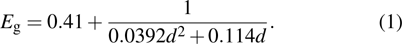
Lead chalcogenide CQDs can also be self-assembled into regular arrays or superlattices (see Fig. 1(d)).[30] In most cases, surfactant molecules such as oleic acid (OA) are coated on the surface of lead chalcogenide CQDs, enabling CQDs to disperse uniformly in varieties of solvents and restrain CQDs from aggregation. The majority of surfactant molecules applied in CQDs' synthesis contain two parts: a long hydrocarbon tail and a polar head. The selection of surfactant molecules depends on the coordination chemistry with CQD surface atoms. According to the Lewis' theory of acids and bases, a hard Lewis acid prefers to bond to a hard Lewis base and this theory can also be applied to the soft Lewis acid and soft Lewis base.[34] Moreover, via capping with different ligands, the position of conduction band (CB) and valence band (VB) in CQDs can be tuned whilst maintaining a constant bandgap.[31] Therefore, the energy level of lead chalcogenide CQD can be tuned to optimize the energy level alignment with types of commonly used charge extraction layers. The effective integration with these layers can obviously enhance the device performances.
3. Fundamentals of CQD photodetectors
3.1. Types of CQD photodetectors
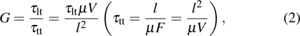
Basically, there are three kinds of CQD photodetectors: photoconductors, phototransistors, and photodiodes.
A typical CQD photoconductor (see Fig. 2(a)) is comprised of a photoactive semiconducting CQD layer and two ohmic contacts integrated with metal to form a two-port optoelectronic device. It works on the principle of a temporary transformation of carrier mobility or density or both in the semiconducting CQD layer when irradiated under incident illumination. The enhancement of conductivity under illumination is most typically ascribed to considerable exciton generation. The mechanism of conductivity in bulk lead chalcogenide film has been extensively studied.[38] Here, we will briefly retrospect the concept of photoconductive gain and the role of trap states in photodetectors based on lead chalcogenide CQD films to interpret the mechanism of photoconductive detectors.

Fig. 2. Schematic images of different device architectures and configurations. (a) A typical photoconductor;[19] (b) a bottom-gate phototransistor;[19] (c) a Schottky photodiode;[35] (d) a heterojunction photodiode;[36] (e) a p–n-type photodiode;[18] and (f) a p–i–n-type photodiode.[37]
Download figure:
Standard imageAn initial current is generated resulting from the absorption of photons, followed by the extraction of photo-generated carriers, which dominates the external quantum efficiency (EQE) of the whole device. This initial photocurrent is the principal source of the photoconductivity. It may also originate from a second photocurrent generated by the injection and the transit of carriers from the electrodes. This second photocurrent dominates the photoconductive gain G, which is expressed as
where τlt is the lifetime of the majority carriers,  is the transit time of the majority carriers, μ is the mobility of the majority carriers, V is the bias voltage, l is the distance between the two electrodes, and F is the electric field arising from bias voltage (F = V/l). Obviously, a gain of
  can be obtained if the device satisfies the condition of
  . Generally, carrier lifetime of a material is adjusted by the existence of hole- or electron-trapping states within bandgap. The trap states in semiconducting materials can be divided into two categories: trapping centers and recombination centers. The former are the traps located in the position close to the band edges, so that the trapped carriers have a great probability to CB or VB under thermal excitation. The latter are the traps located in the position close to the middle of the bandgap, so that the trapped carriers have a great probability to recombine with the opposite charge carriers.[39] Recombination centers can be classified into two kinds by their functions: one can shorten the carrier lifetime (type I centers), while the other one can prolong it (type II or sensitizing centers). The lifetime of a charge carrier in a material with n-type trap states per unit volume with capture cross-section S can be evinced by[39]
where  is the thermal velocity of the charge carriers, Δ E is the energy distance between the trap states and the relative band edge, k is the Boltzmann constant, and T is the temperature. For ligand-exchanged PbS CQD films, the capture coefficient of electrons vS is ∼ 400 times that of holes, thus the electrons are more likely to be captured.[40] Therefore, the photoconductivity in PbS CQD films is predominated by holes. For recombination centers,
  . Additionally, by using the reported figures (
 ,
,  , and
, and  ) and Eq. (3), τtrap can be figured out as ∼ 0.1 ms.[41–43] Consequently, the mid-gap trap states originated from ligand-exchange act as sensitizing centers, and it can prolong the charge carriers' lifetime which depends on the density of traps and the capture cross-section. Based on this mechanism, a net positive or negative charge is left in the photodetector under instantaneous condition, because the majority carriers can be extracted by electrodes but the minority carriers are captured in the trap states. Then, the majority carriers will be injected from electrodes to maintain the neutrality of charges, bringing about the flow of a secondary photocurrent until the whole device has achieved charge balance or recombination occurrence. Systematic and detailed discussion of the implementation of this mechanism on the photoconductors has been investigated.[44–46]
Phototransistors have three metal contacts, as shown in Fig. 2(b). It provides a better control over the conductivity of the semiconducting material, on account of the ability to change the gate voltage, the source-to-drain voltage, and the intensity of illumination. For a p-type lead chalcogenide CQD, considerable holes will be induced by the negative applied bias, thereby increasing the conductivity.[40] The gate electrode acts as a switch which can adjust the position of the Fermi level, leading to the increment or reduction of trap states.
Photodiodes are divided into several categories by the types of junction: Schottky junction (Fig. 2(c)), heterojunction (Fig. 2(d)), p–n junction (Fig. 2(e)), and p-i-n junction (Fig. 2(f)). However, the operating principle for each case is basically the same: separating and collecting the photo-generated electron–hole pairs by building a built-in electric field in junction. During the process of charge extraction, these photo-generated charge carriers need to traverse fairly considerable distances to reach the corresponding electrodes and then to be collected. Therefore, the device thickness is a critical parameter for photodiodes and the lifetime of the charge carriers must be longer than their transit time. The diffusion length of charge carriers in lead chalcogenide CQD films is relatively long and thus can improve the performance of the device. The diffusion length of charge carriers is dominated by not only their mobility but also the average spacing among the recombination centers.[47] Photodiodes can be operated under zero-bias condition (photovoltaic mode), but usually under reverse bias condition (photoconductive mode) which can supply greater bandwidth and wider linear dynamic range. Gain mechanism is also applied to photodiodes by introducing trap-rich material in photoactive region or building heterojunction to capture one type of charge carriers.[48–51]
3.2. Figures of merit
A series of figures of merit are formulated to evaluate the performance of various photodetectors.[52] Firstly, responsibility R(λ) is employed to quantify the electric signal output per optical signal input for photodetectors, and it is defined as the ratio of photogenerated current to optical power of incident illumination on the photodetectors at a specific wavelength λ, thus it is measured in units of A/W. The expression of responsibility is given by
where q is the electron charge, h is the Planckʼs constant, c is the speed of light, ω is the modulation frequency, τ is the time constant, EQE(λ) is the external quantum efficiency, and G is the photoconductive gain.
Another critical parameter which affects the photodetectors' sensitivity is noise. The total noise current in a photodetector consists of four main sources: thermal noise, generation–recombination G–R noise, shot noise, and low-frequency flicker 1/f noise.
For photodetectors, the current signal level produced by incident optical power must be stronger than the noise signal level for the sake of being detected. Considering both the responsibility and the noise, noise equivalent power NEP(λ) is introduced to estimate the sensitivity of photodetectors in noise, and it is defined as the optical power at which the signal-to-noise ratio SNR is unity. NEP(λ) is the minimum optical power that the photodetector can discern per square root of bandwidth. SNR and NEP(λ) are expressed as

where In is the total noise current density, including all the noise sources, and here  presents its root-mean-squared value. R(λ) is the responsibility and P is the incident optical power.
The normalized detectivity or specific detectivity  is the most critical figure of merit for each photodetector, allowing comparison among photodetectors with various configurations and areas.[53] It signifies the SNR when the incident optical power is 1 W, the noise bandwidth is normalized to 1 Hz, and the detector area is 1 cm2.
  is expressed in the unit of
  (Jones) and it is obtained by using the following equation:

where A is the active area of the photodetector. As  is directly proportional to R(λ), it is also an indirect function of applied bias, temperature, modulation frequency, and wavelength. The description of
  for a photodetector should be followed by the measurement condition.
Dynamic range DR(λ) of a photodetector indicates the range over which the photocurrent increases with the incident optical power. DR(λ) is the range of optical power over which the detector can be utilized to detect the incident light. Ideally, R(λ) should maintain constant with the enhancement of optical intensity. DR(λ) is usually reported in the unit of decibel (dB) and expressed as
where  is the maximum incident optical power when the photocurrent saturation arises, and
  is the minimum detectable optical power or NEP(λ). The linear dynamic range implies that the photocurrent increases linearly with the incident optical power.
4. Lead chalcogenide CQDs
In the past decade, photodetectors based on lead chalcogenide CQDs have been widely studied, focusing on PbS, PbSe, and PbSxSe1−x CQDs. As compared to early work of PbS CQD photodiodes pioneered by Sargent group,[54,55] there has been significant promotion in many aspects. The progress of these IR photodetectors is summarized in Table 1.
4.1. Film deposition and ligand exchange
Lead chalcogenide CQDs-based photodetectors are fabricated by spin-coating, dip-coating, or drop-casting techniques on a rigid or flexible substrate, followed by completing a metal electrode. The film conductivity is directly governed by the capping ligands. The carrier transport in CQD films origins from the thermally activated hopping mechanism.[56] The inter-nanocrystal distance dominates the transport, and it depends on the CQD monodispersion and the length of capping ligands. CQDs are typically capped with long and insulated ligands, such as oleic acid (carbon chain length ∼ 2.5 nm)[57–59] and oleylamine (carbon chain length ∼ 2.1 nm).[60] These ligands are essential for CQDs to maintain colloidal stability in organic solvent with low boiling point, but significantly restrain the effective transmission of charge carriers in CQD solids; also, they extend spacing between interfacing dots and lead to low density of QDs.[61] The long, insulated ligands should be exchanged by short, conductive ligands to decrease spacing, and promote film density and electron transport between dots. Another function of capping ligands is to passivate the surface states to reduce the trap state density. It is generally known that there are substantial trap states on the surface of bulk materials due to the presence of dangling bonds. For CQDs, the large surface-to-volume ratios aggravate this effect. Up to date, the most effective and widely-used strategies comprise purely atomic ligands, such as iodine[62–64] and bromine,[4] or a hybrid of atomic ligands and organic ligands with short carbon chain, such as mercaptopropionic acid (MPA)[6] or ethanedithiol (EDT).[65]
Ligand exchange can be divided into two categories: solid-state ligand exchange[7,65,66] and solution-phase ligand exchange.[32,66,67] Figures 3(a) and 3(b) illustrate these two ligand exchange processes. For the solid-state ligand exchange, CQDs capped with long-chain ligands are spin-coated onto the substrate, then a solution containing short-chain ligands such as MPA or EDT is fabricated on the CQD film. In order to wash off exchanged ligands and superfluous short-chain ligands, the as-deposited film is rinsed by a protic solvent followed by a short soaking time and the removal of the solution. Then, the device will be self-assembled by layer-by-layer technique. To ensure the completeness of ligand exchange, the thickness of each CQD layer needs to be controlled by adjusting the concentration of CQD solution.

Fig. 3. (a) Schematic diagram of solid-state ligand exchange and film deposition;[66] (b) schematic diagram of solution-phase ligand exchange and film deposition;[66] and (c) alterable surface dipoles on PbS CQDs via applying various ligands, causing controlled p- or n-type behavior.[68]
Download figure:
Standard imageAs for solution-phase ligand exchange, long-chain ligands are exchanged by short-chain ligands in two orthogonal solvents, then one-step method is employed to deposit ligand-exchanged CQD film. Comparing to the former, the solution-phase process is more facile. However, many factors are needed to consider: the binding among solvent molecules, CQD surface atoms and ligands, and the concentration of CQDs and ligands. Therefore, each part of solvent, CQDs, and ligands needs to be carefully selected and accurately controlled.
Various types of ligands can considerably affect the electrical properties of the CQD film, sequentially affecting the whole performance of photodetectors.[54,69–71] Also, the selection of ligand will directly determine whether the CQDs perform p- or n-type behavior.[7,72] As shown in Fig. 3(c), PbS CQDs capped with EDT show p-type, but they show n-type behavior when they are capped with tetrabutylammonium iodide (TBAI). As described by Milliron,[68] the selection of ligand induces surface dipoles which shift the CB and VB energy level of CQDs, causing them to show p- or n-type behavior, which is also in accordance with Fig. 1(e).
4.2. Lead chalcogenide CQD photodetectors
4.2.1. Lead chalcogenide CQD photoconductors
High G and low noise level are two preconditions for high-sensitivity photoconductors. From Eq. (2), obviously one can see that the majority-carrier lifetime and the majority-carrier transit time play a key role on G. The majority-carrier lifetime can be increased by introducing recombination centers (mid-gap trap states). Other scenarios irrelevant to recombination centers or traps to enhance G are possible; for instance, one kind of the photogenerated carriers are transferred to the high mobility acceptor material while the other kind of carriers stay in the donor material. Sometimes, one kind of charge carriers are trapped in the acceptor material, leaving the other kind of charge carriers to transport, which plays the same effect of arising G. Therefore, the devices can show high G under high electric field if the electrodes replenish the extracted carriers promptly.
Dark current density Jd also plays an important role on device performance since it is a key factor to determine NEP. It mainly depends on the applied electric field, the charge carrier mobility, the type of ligands, CQD dispersity and its size distribution, the band alignment between the metal contacts, and the CB of the photoactive material. Jd can be expressed by[73]
where Nh is the majority carrier (hole) concentration, q is the electron charge, μ is the carrier mobility, and F is the electric field. Most lead chalcogenide photoconductors are fabricated with gold contacts (work function φ=−5.1 eV); in this case, Au can inject holes into the VB of PbS CQDs as its diameter is larger than ∼ 6 nm, and their energy levels are matched. Thus, Nh is considerably increased and the ability of p-type transportation can be enhanced. For PbS CQDs with smaller diameters, only a lower potential barrier for hole injection exists.[32,74]
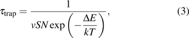
Efforts on suppressing dark current have been made for lead chalcogenide CQD photoconductors. The dark current density can be reduced by two orders of magnitude via blending appropriate proportion of silver nanoparticles (NPs) with PbS CQDs.[73] As shown in Fig. 4, this reduction is due to the introduction of Ag NPs (work function φ=−4.3 eV) as they act as an electron donor and fill almost all shallow electron traps, thus restraining p-type conductivity. In a similar study, electrons are transferred from CB of PbS CQDs to Ag NCs which act as electron traps, prolonging the carrier lifetime and enhancing the photocurrent up to three orders of magnitude.[75]

Fig. 4. (a) Architecture of a PbS-CQD:Ag NP photoconductor;[73] (b) Ag NPs act as an electron donor, which would be capable to apply electrons to system and thus to modify the density of charge carriers;[73] (c) a gradual change from p-type to intrinsic and n-type behavior with increasing Ag NPs (w/w) concentration;[73] (d) the dark current density for different PbS-CQDs:Ag NP blends.[73]
Download figure:
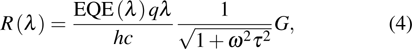
Standard imageUsually, the as-synthesized PbS CQDs are p-type. Therefore, electron–hole pairs are generated in the PbS CQD film under illumination and the majority of photocurrent is holes. As shown in Fig. 5(a), there are two different pathways for excited electrons: they are directly excited to mid-gap states (Mx and M1s) or directly to CB states (1Sh to 1Se). Also, the trapped electrons in mid-gap states can be further excited to CB states. The majority of photocurrent originates from the transitions of Mx and M1s, which are more dominant than the intrinsic band edge transitions (see Fig. 5(b)). The intrinsic band edge transitions can be seen at longer wavelengths according to the excitation energy of mid-gap states. For ligand-exchanged lead chalcogenide CQD photodetectors, R(λ) is dominated by the occupation of mid-gap states, and it depends on the incident light intensity. Trap states dominate under low illuminating intensity, and their density is higher than the photo-generated charge carriers; in this way, holes transit while electrons are trapped or partly fill mid-gap states, thus leading to high G. On the contrary, the trap states will be gradually filled as the incident light intensity increases, resulting to the increment of electrons' quasi-Fermi level, and the gain will be lower. From Eq. (2), it is obvious to see that G is proportional to the applied bias, and an unlimited G can be obtained for a high applied bias (provided that the bias is lower than the device breakdown voltage). However, there is a critical limit: the fast recombination of charge carriers is induced by the growing density of charge carriers filled in the trap states; in this way, the carrier lifetime will decrease and then G will be reduced. Therefore, the maximum G is related not only to the incident light intensity, traps density, and position, but also to the applied bias.

Fig. 5. (a) PbS CQD energy level diagram depicting the transitions between the quantized energy levels and mid-gap band (MGB) trap states (red arrows);[40] the red/blank circles represent electrons/holes, the wavy black arrows represent the relaxation pathways, and the blue arrow marks the position of Fermi level; (b) EQE as a function of incident photon energy under different gate biases;[40] the energy spacing between two highlighted features M1s and Mx is 0.6 eV, corresponding to half of the energy spacing between the 1S and X features in the absorption spectrum (inset).
Download figure:
Standard imageAs described above, there is a conflict between G and the transient response, and there is a fundamental trade-off between G and bandwidth. A feasible approach to this challenge is to introduce a bimolecular interfacial recombination process in devices.[76] This photoconductor was fabricated by employing a [6,6]-phenyl-C61-butyric acid methyl ester (PCBM) layer on top of PbS CQD layer. When the device is illuminated, photo-generated electrons transfer from PbS CQD to PCBM, and then recombine with holes at PbS-CQD/PCBM interface. As the hole mobility in PbS film is low ( ), this bi-layer configuration decreases the carrier lifetime of PbS CQDs and avoids the trap-assisted recombination. A bandwidth
  can be realized under the incident light intensity of 57 mW/cm2.
Type-II heterojunction based organic-inorganic hybrid photoconductors were reported via blending lead chalcogenide CQDs with fullerene acceptors, such as PCBM,[77] C60 crystals,[78] and C60 nanorods (NRs).[79] A highlighted merit of hybrid devices is that they can operate under the condition of CQDs capped with long-chain ligand, such as OA. In this case, the photo-generated charge carriers transport through the doping acceptor materials, despite that the long-chain ligands can suppress the transport of electrons. Both types of charge carriers can be extracted by electrodes in these devices, depending on the type of ligands and the charge percolation pathways. Supposing the electron transportation occurs from CQDs to PCBM, then the diameter of the synthesized CQDs needs to be strictly controlled to make the CB level of CQDs consistently higher than the lowest unoccupied molecular orbital (LUMO) of PCBM (3.7 eV–4.3 eV).[80] Therefore, the application of PCBM for wavelength shorter than ∼ 1400 nm is limited.[81] As a substitution of PCBM, C60 was used due to its lower LUMO (∼ 4.5 eV), and it can accept electrons from larger diameter CQDs. It has been confirmed that R(λ) of devices employing C60 responses up to ∼ 2000 nm.[82] Related studies with various organic and inorganic charge acceptor materials have been presented.[83] Moreover, CQD-based photoconductors incorporating with 1D nanomaterials were fabricated,[79] which benefit from large donor/acceptor interfaces. Also, devices by making good use of surface plasmons have been carried out.[84–86]
4.2.2. Lead chalcogenide CQD phototransistors
From Eq. (2), one can see that G is directly proportional to the mobility of charge carriers, thereby the hybrid phototransistors are generally fabricated by integrating lead chalcogenide CQDs with high mobility materials, such as polymers[57,58,87,88] or two-dimensional materials[89–92] or both.[93]
Poly(3-hexylthiophene) (P3HT) is the most widely used p-type polymer which possesses the highest hole mobility ( ) among the reported polymers.[94,95] Accordingly, it is reasonable to blend lead chalcogenide CQDs with P3HT to promote hole transport. Wang et al.[58] reported a hybrid PbSe-CQD:P3HT (2:1 wt%)-based phototransistor with R(λ) of 500 A/W and
  of 5.02×10¹² Jones. Song et al.[88] reported a hybrid PbS0.4Se0.6-CQD:P3HT (2:1 wt%)-based phototransistor with R(λ) of 5.6×10⁻² A/W and
  of 1.02×10¹⁰ Jones. Under illumination, photo-generated holes transfer from CQDs to P3HT while photo-generated electrons are trapped in CQDs. The transfer of holes is rapid under the applied electric field due to the high mobility of holes in P3HT, which significantly decreases the transit time of holes, leading to high G. Konstantatos et al.[90] have introduced mechanically exfoliated single/bilayer graphene flakes into PbS CQD-based phototransistor, realizing relatively high R(λ) and
  of 107 A/W and 7×10¹⁷ Jones, respectively. The effective detectable optical powers for this hybrid device can fall to ∼ 10 fW, exhibiting a slow rise time of ∼ 10 ms and a bi-exponential decay time of ∼ 100 ms and ∼ 2 s. The decay time can be decreased by applying a gate voltage to reduce the potential barrier at PbS-CQD/graphene interface by maintaining the electrons captured in the CQDs, and its R(λ) can be enhanced by ligand exchange techniques: an ultra-high
  can be achieved by applying thioglycerol (TGL)/dithioglycerol (DTG) ligands.[91] It is worthwhile to mention that the trade-off between G and bandwidth has been conquered via establishing a photo-junction field-effect transistor (photo-JFET).[96] Such a kind of device has been fabricated by depositing a transparent conductive molybdenum trioxide (MoO3) layer on top of a moderately n-type PbS CQD layer to form a rectifying junction. The photo-JFET can achieve G of 10 at modulation frequency of 100 kHz, whereas those photoconductors employing PbS CQDs generally exhibit G below 100 Hz. G of lead chalcogenide CQD:two-dimensional material hybrid phototransistors have exhibited several orders of magnitude larger than that of CQD-only based photoconductors. As compared with photoconductors, phototransistors focus on decreasing the transit time of charge carriers instead of prolonging their lifetime, although both can enlarge G.
4.2.3. Lead chalcogenide CQD photodiodes
As mentioned above, photodiodes can be divided into several categories according to the types of junction. The Schottky-type photodiodes are fabricated by constructing a rectifying junction at proper metal/semiconductor interface, building an built-in electric field to extract the charge carriers efficiently. Clifford et al.[35] reported a Schottky-type photodiode with a configuration of indium-tin oxide (ITO)/PbS-CQDs/aluminum (Al). The PbS-CQDs form ohmic contacts with both ITO and Al. This device exhibited a bandwidth of 3 dB at modulation frequency  . Moreover, CQD:polymer nanocomposites have also been applied in this type of photodiodes. A PbS-CQD:P3HT single nanowire (NW) hybrid device has been fabricated with a competitive
  of 2.1×10¹² Jones, using Schottky contacts and OA-capped PbS CQDs as the active layer.[97]
The heterojunction photodiodes are fabricated by constructing a semiconductor/semiconductor junction to extract the charge carriers efficiently; it is typically structured by means of cooperating lead chalcogenide CQDs with n-type semiconductor, and π-conjugated polymers are also feasible in some cases. The selection of materials should satisfy the band alignment of the devices, i.e., it can promote the extraction of both holes and electrons at their corresponding contacts. An organic-inorganic hybrid photodiode was reported by blending OA-capped PbS CQDs with P3HT and PCBM.[98] The introduction of P3HT and PCBM prompts efficient transport of holes and electrons from CQDs, respectively, exhibiting an EQE of 51% and  of 2.3×10⁹ Jones. Dong et al.[99] introduced zinc oxide (ZnO) nanoparticles into the PbS-CQDs:P3HT:PCBM blend film, and the device showed an EQE of 1624% and
  of 2.2×10¹¹ Jones. The high trap density in metal oxides can availably trap the photo-generated electrons, triggering holes injection via electrodes from the external circuit.
The p–n junction photodiodes are fabricated by integrating p-type lead chalcogenide CQDs with wide-bandgap n-type metal oxides to form a p–n junction. The most commonly adopted metal oxides are ZnO[59] and titanium dioxide (TiO2).[100] ZnO/TiO2 as an electron-transporting layer was introduced by Pal et al.[18] The dark current of this device is two orders of magnitude lower than that of Schottky-type photodiodes. Sulaman et al.[59] reported a photodiode employing ZnO nanoparticles as an interlayer between ITO and PbS0.4Se0.6 CQD layer, and it displayed a competitive  of 1.3×10¹³ Jones under
  980 nm laser illumination. Afterwards, Sulaman et al.[101] reported a broadband photodiode by epitaxially blending CH3NH3PbBr3 CQDs with PbS0.4Se0.6 CQDs as the active layer, and it exhibited a maximum R(λ) and
  of 21.48 A/W and 3.59×10¹³ Jones, 22.16 A/W and 3.70×10¹³ Jones at room temperature under
  532-nm laser and
  980-nm laser illumination, respectively.
Also, the p–i–n-type photodiodes have been reported with an ultra-high G (maximum EQE( ) and a high
  of 7×10¹³ Jones in these years.[37,102] This type of photodiode integrates both electron- and hole-blocking layer in one device to inhibit the charge carrier injection via the electrodes from the external circuit, as shown in Fig. 6. The Fermi level of PbS CQDs will be reduced and close to the intrinsic level after ligand treatment with 1,3-benzenedithiol. Therefore, PbS CQD layer can be treated as an intrinsic semiconductor layer and it is sandwiched between p-type layer (1,1-bis[(di-4-tolylamino)phenyl]cyclohexane (TAPC)) and n-type layer (ZnO). It is worth noting that EQE(λ) surpasses 100%, and it results from not only the primary photocurrent but also the secondary photocurrent. A photoconductive process occurs due to the charge carrier injection from electrodes under illumination and applied bias. Therefore, the transient response of p–i–n-type photodiodes is slow, and it is usually in ms (similar to that of photoconductors). The high
  in these devices is due to the generation of secondary photocurrent (instead of a low noise level). However, for Schottky-type photodiodes and p–n-type photodiodes, a low noise level is expected which allows the device to be operated under zero-bias condition, although a slight reverse bias will obviously elevate both the EQE(λ) and bandwidth. Further efforts can be done via optimizing the thickness of active layer to make it adequately depleted, and meanwhile, constructing potential barriers with proper height to efficiently inhibit the charge carrier injection from electrodes.

Fig. 6. (a) Schematic cross-section view of a p–i–n type photodiode;[37] (b) schematic energy band diagrams of a p–i–n type photodiode in the dark (left panel) and under IR illumination (right panel);[37] (c) EQE(λ) values as function of wavelength under reverse bias (left panel), and  values as function of wavelength under reverse bias (right panel);[37] (d) light intensity dependence of EQE(λ) (left panel) and
  (right panel) at a constant bias of 10 V.[37]
Download figure:
Standard image4.2.4. Tandem photodetector
To further enhance the performance of photodiodes, tandem structure was introduced to suppress the high dark current. Compared with single-layer architecture, the unique advantage of tandem architecture is that the intermediate layer functions as a valid energy barrier which suppresses the dark current; meanwhile, photocurrent is harvested through effective charge carrier recombination at the intermediate layer. The dominant electrical transport mechanism is altered from carriers hopping between the nearest CQD units to the charge carrier recombination at the intermediate layer, and thus the CQDs are no longer the dominant limiting factor for the performance of photodiodes. In 2015, a PbSe CQDs-based tandem photodetector glass/ITO/PEDOT:PSS/PbSe/ZnO/poly-TPD/PbSe/ZnO/Al was reported by Jiang et al.,[103] in which ZnO as a hole-blocking layer (HBL) and poly-TPD as an electon-blocking layer (EBL) were employed as the intermediate layers (see Fig. 7(a)) to serve as the recombination centers for electrons from one sub-detector and holes from the other sub-detector. The measured dark current of tandem photodetector showed a significant reduction of more than three orders of magnitude as compared with that of the photodetector with single-layer architecture, as shown in Fig. 7(b). And the tandem photodetector exhibited quite high  of 4.7×10¹³ Jones and 8.1×10¹³ Jones under
  1100-nm laser illumination, respectively, at 275 K and 100 K. Recently, our research group presented a high-performance tandem photodetector via employing blends of PbS0.4Se0.6 CQDs and CsPbBr3 CQDs,[101] and found the dark current can be further reduced by introducing a poly(methyl methacrylate) (PMMA) dielectric layer between the two sub-detectors, i.e., ITO/PEDOT:PSS/CsPbBr3:PbS0.4Se0.6/ZnO/PMMA/PVK/CsPbBr3:PbS0.4Se0.6/ZnO/Au, and it exhibited a high R(λ) of 27.72 A W−1 and an ultra-high
  1.32×10¹⁴ Jones under
  980-nm laser illumination. Also, other crucial parameters of the tandem photodetector with PMMA interlayer are summarized in Table 2.

Fig. 7. (a) Device configuration and band diagrams of single-layer photodetector and tandem photodetector; (b) current density–voltage (J–V) characteristics in dark (Jd) and under illumination (Jph) of single-layer photodetector and tandem photodetector.[103]
Download figure:
Standard imageTable 2. Parameters obtained for tandem photodetector with PMMA interlayer.[101]
| Laser wavelength/nm | Illumination intensity/ |
Responsibility/(A/W) | Detectivity/Jones |
|---|---|---|---|
| 520 | 43.5 | 20.61 | 9.87×10¹³ |
| 650 | 49.8 | 18.87 | 9.04×10¹³ |
| 780 | 50 | 17.33 | 8.30×10¹³ |
| 980 | 57.8 | 27.72 | 1.32×10¹⁴ |
| 1050 | 55 | 18.95 | 9.07×10¹³ |
4.2.5. Lead chalcogenide CQD-based IR detecting and display devices (IR-DDD)
Based on the development of IR detectors, IR imaging devices have recently harvested quantities of attention owing to their wide range of applications, such as night vision,[104] national defense,[105] and biomedical research.[106] The conventional IR imaging system is generally realized by interconnecting IR focal plane detector arrays with read-out circuits via indium bumps.[107] However, there are a series of limits on this technology, i.e., high cost, time-consuming, complicated techniques, and restricted detectable IR wavelength range. To solve these challenges, optical up-conversion technology has been proposed and developed as an alternative method,[108] and we have called it as IR-DDDs for such a kind of up-conversion devices.[108]
An IR-DDD commonly consists of two categories: with light-emitting diode (LED) and without LED. The former device integrates a detecting unit (photodetector) with a display unit (LED or organic LED (OLED)). The free charge carriers are generated by the incident light in the active layer of photodetector, subsequently these charge carriers inject into display unit and ultimately emit light in the light-emitting layer, of which the emission wavelength is shorter than the incident light.[110,111] The latter device possesses a nonlinear optical process, in which the device absorbs two or more incident photons via the intermediate long-lived energy states, and emit light with a shorter wavelength.[112] Compared to the latter, the emission wavelength in visible region can be more easily chosen in the former device, as the emission wavelength of the former is independent of the incident wavelength.
With the rapid development of organic electronics, OLEDs have drawn widespread interest due to their unique advantages: low cost, easy to realize large-area fabrication and flexibility; in addition, they are no longer restricted by the properties of substrates and lattice matching principle. Therefore, OLEDs have been increasingly employed as the display units in IR-DDDs.[113–115]
Lead chalcogenide CQD-based IR-DDD generally interconnects a lead chalcogenide CQD-based photodetector as an IR detecting unit and a high-efficiency phosphorescent OLED as a display unit. It is worth mentioning that the configuration of photodetector in IR-DDD transforms from p–i–n-type photodiode[115] to heterojunction field-effect phototransistor (HFEPT)[116] to further enhance the performance of IR-DDD, as it exists high internal G and can realize the photocurrent amplification. In 2011, So et al.[117] firstly reported an IR-DDD integrated with PbSe CQD sensitizing layer and a phosphorescent OLED. The photon-to-photon conversion efficiency for this device (from 1300 nm to 520 nm) is about 1.3%. They adopted a broad-bandgap ZnO layer as the hole-blocking layer, and it increased the threshold voltage in the dark and decreased the dark current obviously, thus enhancing the SNR. However, its response range in IR region is only from 1000 nm to 1500 nm and significantly limits its detection range. In 2016, So et al.[109] reported their latest results on PbS CQD-based vertical field-effect phototransistor (VFEPT) (see Fig. 8), in which a perforated metallic source electrode was employed. This VFEPT showed an EQE up to 1×10⁵% with a  of 1.23×10¹³ Jones under
  1042-nm laser illumination. After incorporating a phosphorescent OLED into the VFEPT, an IR-DDD is constructed and its average photon-to-photon conversion efficiency (from 1043 nm to 550 nm) is 1597% at an IR power density of
  .
.

Fig. 8. IR-DDD configuration consisting of a PbS CQD-based VFEPT and a phosphorescent OLED, in which a porous ITO layer is used as the source electrode.[109]
Download figure:
Standard imageIn a word, IR-DDDs represent a promising subject when it gets a high inner-gain, and might lay the foundation for new emerging optoelectronic devices for infrared imaging.
5. Conclusion
A great success has been achieved by introducing lead chalcogenide CQDs for IR photodetectors. During the past decade, it is fairly promising for lead chalcogenide CQD-based IR photodetectors on account of facile implementation at room temperature, low cost, flexible substrate compatibility, and high figure of merit. In order to further promote device performance and reach commercialization, there are still several challenges that need to be solved. For example, controlling the synthesis process of CQDs to enhance the stability of CQDs, understanding how the CQD size affects the optoelectronic properties of the devices, CQD ligand exchange techniques, surface charge transfer between CQDs, and comprehensive diagram of charge carrier transport along with the manipulation of the trap states or charges in CQD films. With the recent progress of advanced technologies, these problems would be solved. Although currently there are some challenges, we still firmly believe that lead chalcogenide CQD-based photodetectors possess further potential in the continuous improvement for each figure of merits.
Footnotes
- *
Project supported by the Fund from the State Key Laboratory of Transducer Technology, China (Grant No. SKT1404) and the Fund from the Key Laboratory of Photoelectronic Imaging Technology and System (Grant No. 2017OEIOF02) at Beijing Institute of Technology, Ministry of Education of China.