
Abstract
We present a systematic study on the effects of CF4 plasma immersion ion implantation (PIII) in Si on the phase evolution of ultra-thin Ni silicides. For 3 nm Ni, NiSi2 was formed on Si substrates with and without CF4 PIII at temperature as low as 400 °C. For 6 nm Ni, NiSi was formed on pure Si, while epitaxial NiSi2 was obtained on CF4 PIII Si. The incorporation of C and F atoms in the thin epitaxial NiSi2 significantly reduces the layer resistivity. Increasing the Ni thickness to 8 nm results in the formation of NiSi, where the thermal stability of NiSi, the NiSi/Si interface and Schottky contacts are significantly improved with CF4 PIII. We suggest that the interface energy is lowered by the F and C dopants present in the layer and at the interface, leading to phase evolution of the thin Ni silicide.
Export citation and abstract BibTeX RIS

Original content from this work may be used under the terms of the Creative Commons Attribution 3.0 licence. Any further distribution of this work must maintain attribution to the author(s) and the title of the work, journal citation and DOI.
1. Introduction
NiSi is used as Ohmic or Schottky contacts at the source/drain and gate in metal-oxide-semiconductor field effect transistors (MOSFETs) because of its low resistivity, low thermal budget and silicon consumption [1–3]. Ultra-thin silicide layers with high uniformity are required for scaled nanometre devices. However, the instability of NiSi due to low transition temperature to highly resistive NiSi2 phase and grain agglomeration, especially for very thin layers at high temperatures, results in rough interface and surface, causing non-uniform contacts and substantial leakage at shallow junctions [4–6]. The thermal stability of the NiSi layer has been improved by incorporating elements such as Pt [7, 8], C [9, 10] and F [11] in Ni or silicon substrate or adding a new thin layer [12, 13]. With these methods the thermal stability of NiSi was increased at least 100 °C by inhibiting the agglomeration of NiSi grains and delaying NiSi2 nucleation.
The solid-state reaction of Ni with a Si substrate leads to the sequence phase formation of δ-Ni2Si, NiSi and NiSi2. High resistivity phase NiSi2 forms at an annealing temperature normally higher than 700 °C [14–17]. The interface energy plays an important role in phase evolution, especially when the film thickness is very thin [18, 19]. The phase formation sequence can be changed with a decrease of film thickness. Recent reports showed that when the thickness of the deposited Ni film is less than 4 nm, epitaxial NiSi2 layers with high single crystalline quality and high thermal stability are formed even at low temperatures (300 °C) [20–23]. During the silicidation process, no NiSi phase is observed, but epitaxial θ-Ni2Si mesophase is found before the formation of epitaxial NiSi2 [22]. The epitaxial NiSi2 layer with an atomic flat NiSi2/Si interface shows super properties and has been used for advanced nanometre transistors [24–26]. The thickness of the epitaxial NiSi2 is limited to <10 nm due to the limited Ni thickness (<3 nm). Moreover, when the thickness of the Ni film is less than 6 nm, θ-Ni2Si replaces δ-Ni2Si as the first phase during silicidation [22]. The phase evolution can also be changed by additive elements especially in very thin films. For example, epitaxial θ-Ni2Si instead of δ-Ni2Si was obtained as the first phase by silicidation of Ni-Pt alloy with Si [27–29]. Geenen et al [30] discovered a broader temperature range for δ-Ni2Si formation and low-temperature NiSi2 formation with 10% Co in 9 nm Ni. They also concluded that the NiSi formation is delayed by 10% Al doped in 9 nm Ni. However, for silicidation with C and F incorporations, only the phase formation behaviour was investigated in the case of thick films [9–11]. It should be very interesting to investigate the phase evolution of nickel silicide in the ultra-thin films combining the effect of C and F elements.
This paper presents the phase evolution of Ni silicides with different Ni thicknesses (3 nm, 6 nm and 8 nm) on CF4 plasma pre-implanted Si (100), aiming to study the impact of Ni thickness and the effects of C and F impurities on the phase evolution. This enables us to obtain a comprehensive understanding of silicide formation as a function of film thickness and the effects of impurities.
2. Experimental
Figures 1(a)–(c) show the silicidation process. In this work, 300 mm p-type silicon (100) wafers were used as substrates. Firstly, CF4 plasma immersion ion implantation (PIII) was applied using PULSION plasma implanter developed by Ion Beam Services (IBS) into Si substrates (figure 1(a)) at room temperature at a plasma energy of 2.5 keV to a fluence of 5 × 1015 cm−2. The distributions of C and F in Si measured by secondary ion mass spectrometry (SIMS) were presented in figure 1(d). It showed very high density of C and F atoms with peak concentrations of ∼2 × 10²¹ C cm−3 and ∼6 × 10²¹ F cm−3 in Si within a depth of 20 nm. The F peak is located at a depth of ∼3 nm. CF4 PIII offers high efficiency to introduce a high concentration of C and F atoms closer to the surface than the beamline ion implantation.
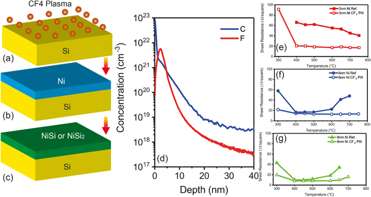
Figure 1. (a)–(c) Silicidation process on CF4 PIII treated Si(100) substrates; (d) SIMS profiles of C and F in Si after CF4 PIII; (e)–(g) sheet resistance of nickel silicide layers formed with 3 nm, 6 nm and 8 nm Ni, respectively, showing the thermal stability of the silicide layers. The reference samples represent the layers formed on Si(100) without CF4 PIII.
Download figure:
Standard image High-resolution imageSubsequently, these wafers were cut into small pieces for further processing. After removing the native SiO2 in 1% HF solution, Ni layers with different thickness (3 nm, 6 nm and 8 nm) were deposited onto the Si substrate by sputtering (figure 1(b)). Then the silicidation process was carried out with rapid thermal annealing (RTA) for 10 s at different temperatures ranging from 300 °C to 750 °C in forming gas (96% N2 and 4% H2) (figure 1(c)). Finally, the unreacted Ni was removed with H2SO4:H2O2 (4:1) solution.
The fabricated silicide layers were characterized with different techniques. The thermal stability was detected by van der Pauw resistance measurements. The morphologies of the layer and the silicide/silicon interface were investigated by transmission electron microscope (TEM). Rutherford backscattering spectrometry (RBS) was used to measure the silicide composition and thickness. The distribution of elements in the sample was measured by SIMS.
3. Results
Because of the large difference in resistivity between NiSi and NiSi2, the sheet resistance measurement could offer a reliable way to study the phase formation. Figures 1(e)–(g) show the thermal stability of the silicide layers by plotting the sheet resistance as a function of silicidation temperature for silicides formed with 3 nm, 6 nm and 8 nm Ni, respectively. Reference samples without PIII are shown for comparison.
3.1. Silicide formed with 3 nm Ni
For the silicide layers formed with 3 nm Ni, the sheet resistance value remains almost constant with the annealing temperature from 400 °C to 750 °C, as shown in figure 1(e). It has already been reported that an epitaxial NiSi2 layer was formed on Si (100) when the Ni layer is <3 nm [20]. Experimental results presented in this paper for the 3 nm Ni reference sample are consistent with the published results. In addition, the RBS channelling measurements indicate that a single crystalline NiSi2 layer with a thickness of ∼9 nm was formed on the PIII samples, as indicated in figure 2(b). The cross section TEM image in figure 2(a) further shows an epitaxial NiSi2 layer with a flat surface. However, pyramids with wedge-shaped (111) facets in some regions were observed at the interface, which resulted from the lower surface energy of (111) surfaces. Surprisingly, the sheet resistance of the NiSi2 layer formed on CF4 PIII Si substrate is much lower than the reference sample. At a silicidation temperature of 500 °C, the sheet resistance of the NiSi2 layer formed on CF4 PIII Si substrate is only 18.7 Ω/□, corresponding to a specific resistivity of 16.8 μΩ cm which is comparable to the value of NiSi, while the reference sample shows a sheet resistance of 61.9 Ω/□ for a specific resistivity of 55.7 μΩ cm. The lower resistivity with CF4 should be related to the C and F incorporation in the NiSi2 layers. We found that C atoms and part of the F atoms distribute in the NiSi2 layer (see also figure 7 for 6 nm Ni), which may reduce the point defects in the layer, similar to the behaviour found for NiSi [9]. The effects of C and F in the layer for the low resistivity are still not very clear and requires more investigation. In addition, at a higher silicidation temperature of 750 °C, the epitaxial layer with perfect uniformity and atomic flat surface/interface was achieved, as indicated in figure 2(c).
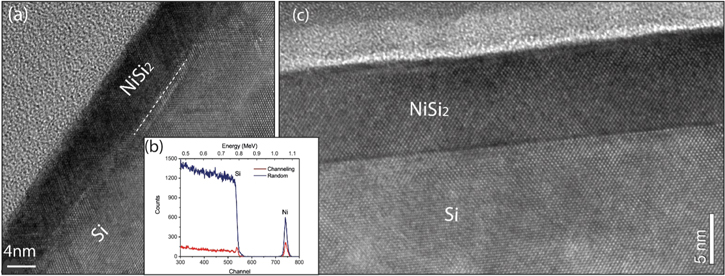
Figure 2. (a) Cross section TEM image for the NiSi2 layer formed with 3 nm Ni on CF4 implanted Si (100) at 500 °C. (b) The RBS random and channelling spectra for the NiSi2 layer formed at 400 °C on the CF4 implanted Si (100) substrate, showing an epitaxial NiSi2 layer on Si (100). (c) A TEM image shows high quality epitaxial NiSi2 layer with an atomic flat NiSi2/Si interface formed at 750 °C.
Download figure:
Standard image High-resolution image3.2. Silicide formed with 6 nm Ni
For 6 nm Ni samples, a much larger thermal stability window is found for the layers formed on PIII treated substrates, as shown in figure 1(f). Figure 3(a) shows the RBS random and channelling spectra for the Ni silicide layers formed with 6 nm Ni at 450 °C. It is clearly seen that a NiSi layer with a thickness of ∼12 nm was formed on pure Si (100) without PIII, which is indicated by the higher Ni signal in the RBS spectrum (green). However, the RBS channelling spectrum indicates that an epitaxial NiSi2 layer with a thickness of ∼19 nm was formed on CF4 PIII Si (100) at 450 °C. The single crystalline NiSi2 layer shows higher thermal stability than the NiSi layer as shown in figure 1(f). At 450 °C, the NiSi2 layer shows a sheet resistance of 14.2 Ω/□ corresponding to a specific resistivity of 27 μΩ cm, which is higher than the layer formed with 3 nm Ni due to more defects, as compared by the TEM images in figures 2 and 3, but lower than the NiSi2 layer formed with 3 nm Ni on the reference sample. The reference NiSi layer has a sheet resistance of 17 Ω/□ for a resistivity of 20.4 μΩ cm. The NiSi layer formed on pure Si suffers agglomeration at temperatures >600°C, thus causing the degradation of sheet resistance.
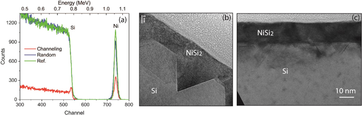
Figure 3. (a) RBS random and channelling spectra for the Ni silicide layer formed with 6 nm Ni at 450 °C on CF4 implanted Si, showing an epitaxial NiSi2 layer. However, the RBS spectrum (green) for the reference sample shows a NiSi layer formed on pure Si (100). (b), (c) Cross sectional TEM image for NiSi2 formed on CF4 implanted Si (100) with 6 nm Ni after annealing at (b) 500 °C, and (c) 650 °C. The NiSi2/Si interface is improved with high temperature.
Download figure:
Standard image High-resolution imageFigures 3(b) and (c) show the cross section TEM images for NiSi2 layers formed with 6 nm Ni layer at silicidation temperature of 500 °C and 650 °C, respectively. The comparison of these two TEM images shows that the NiSi2 (111) facets for the layer formed at 650 °C annealing temperature is less than that at 500 °C, indicating that higher annealing temperature is needed for higher single crystalline quality of the NiSi2 layer, which is similar as the case of 3 nm Ni. The formed NiSi2 layer shows much better surface compared to the NiSi layer formed on pure Si(100) substrate due to the single crystallinity.
X-ray reciprocal space mapping (RSM) measurement further shows that the NiSi2 layer grows psuedomorphically and a forms single crystal on the CF4 PIII silicon substrate with tensile strain, as demonstrated in figure 4. NiSi2 has a cubic structure with a lattice constant of 5.406 Å [31]. However, the lattice constant of NiSi2 in the surface perpendicular direction is about 5.37 Å, smaller than the value in the reference. Due to the relatively low single crystalline quality and thin layer of NiSi2, the NiSi2 signal is not sharp compared to the Si substrate signal. The incorporation of C and F in the NiSi2 layer and the relatively low single crystalline quality could cause a smaller measured lattice constant of NiSi2 in the surface perpendicular direction.
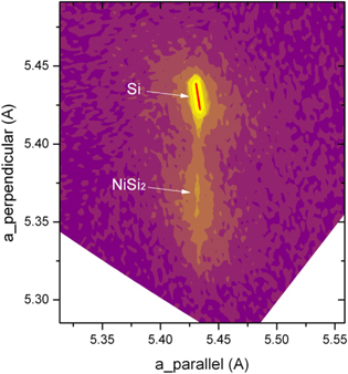
Figure 4. X-ray RSM for NiSi2 formed with 6 nm Ni at 450 °C on CF4 PIII Si (100), showing lattice constant of 5.37 Å for NiSi2 in the surface perpendicular direction and the same lattice constant as Si (100) (5.43 Å) in plain, thus causing a biaxial tensile strain in NiSi2.
Download figure:
Standard image High-resolution image3.3. Silicide formed with 8 nm Ni
From the RBS measurements (not shown) for 8 nm Ni samples, we found that ∼15 nm thick NiSi layers were formed on both the pure Si and CF4 PIII Si substrates at silicidation temperatures ranging from 400 °C to 650 °C. Figure 5 shows cross section TEM images for the NiSi layers formed on Si substrates with and without CF4 PIII. The NiSi/Si interface is much smoother on the CF4 PIII Si substrate, which leads to an increase of the thermal stability of NiSi as shown in figure 1(g).
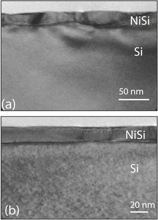
Figure 5. Cross section TEM images of silicide layers formed with 8 nm Ni on (a) pure Si (100) for reference; and CF4 PIII treated Si (100) (b), showing improved layer uniformity and smoother NiSi/Si interface for the CF4 PIII sample.
Download figure:
Standard image High-resolution imageTable 1 summarizes the Ni silicide phase formed on Si (100) at a temperature range from 400 °C to 650 °C, in which all the layers are thermally stable as shown in figures 1(e)–(g). From table 1, we can see that CF4 PIII increases the critical thickness of Ni for direct formation of NiSi2 from 3 nm to 6 nm. Figure 6 displays the phase evolution and the corresponding specific resistivity for silicides formed at 500 °C on Si substrates with and without CF4 PIII. It is very interesting that the NiSi2 layer formed with 3 nm Ni on CF4 PIII Si substrate shows a very low resistivity which is comparable and even lower than that of NiSi formed with 6 and 8 nm Ni on pure Si substrates. This is a big advantage for applications because the epitaxial NiSi2 is much more stable and uniform.
Table 1. Summary of silicide phase on Si (100) with and without CF4 PIII.
| Ni thickness | w/o CF4 PIII | With CF4 PIII |
|---|---|---|
| 3 nm | NiSi2 | NiSi2 |
| 6 nm | NiSi | NiSi2 |
| 8 nm | NiSi | NiSi |
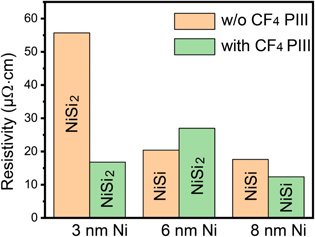
Figure 6. Summary of the phase evolution and corresponding specific resistivity for silicides formed at 500 °C with different Ni thicknesses.
Download figure:
Standard image High-resolution image4. Discussion
It is known that the growth kinetics of NiSi2 is nucleation controlled, while NiSi is controlled by diffusion with Ni as the diffusing specie [15, 16]. However, when the initial Ni film is thinner than 4 nm, reactions are no longer limited by atomic diffusion [19, 32, 33]. Interface energy plays a vital role for ultra-thin films. Consequently, epitaxial NiSi2 instead of polycrystalline NiSi is formed at low temperatures (400 °C). From the nucleation theory the silicide phase should be formed with a larger Gibbs free energy ( ) reduction which is given by [34]:

where  is the interface energy change in which the grain boundary energy and the interface energy changed by strain are included.
  is the free energy difference in volume and
  is the enthalpy change, T is the temperature, and
  is the entropy difference. Since
  is usually very small,
  for both NiSi and NiSi2 phase can be written as the following:


where t is the thickness of the Ni film. The factors 2.01 and 3.59 are the corresponding silicide/Ni thickness ratio [31]. The heat of formation ΔH for NiSi and NiSi2 are −10.3 kcal/mol.at and −7.2 kcal/mol.at, respectively [35]. Taking the molecular density of 4.552 × 1022 cm−3 for NiSi and 2.457 × 1022 cm−3 for NiSi2 into account we can obtain  −0.78 kcal cm−3.at and
  −0.29 kcal cm−3.at. In addition,
  is usually less than
  due to the epitaxy of NiSi2. Therefore we can conclude
  favoring the NiSi formation when t is larger, as demonstrated schematically by solid lines in figure 8. For a very thin Ni layer, the interface energy (
 ) contributes more to
  according to equations (2) and (3), which means
  when the film thickness is less than a critical thickness t1. The epitaxial atomic alignment of NiSi2 reduces the interfacial energy and is thus energetically favourable for its formation for a small thickness of Ni film.
It is likely that dopants like C and F change the silicide formation behaviour by affecting the interfacial energy. Figure 7 shows the SIMS profiles of C and F in NiSi2 formed with 6 nm Ni. It is found that the distribution of C atoms is almost independent of silicidation temperature. More F atoms segregate at the interface by increasing temperature, as indicated by the higher F peak at the NiSi2/Si interface. F segregation results are also found for other samples with different Ni thicknesses (not shown). Most C, and a portion of F atoms, exist in the silicide, refining the grain boundaries of silicide and reducing the defects. A large density of F atoms segregate at the silicide/Si interface, which enhances the interface cohesion and makes the interface smoother [9–11]. Therefore, for the formation of NiSi2 with 3 nm Ni, CF4 PIII caused a lower density of the pyramids at the interface and decreased the sheet resistance of NiSi2. For the formation of NiSi with 8 nm Ni, the smoother surface and interface increase the nucleation barrier of NiSi2 and thus enhance the thermal stability of NiSi [36].

Figure 7. SIMS profiles for C and F atoms in the NiSi2 layers formed at 450 °C and 750 °C with 6 nm Ni on CF4 PIII Si(100), showing F segregation at the NiSi2/Si interface. The increasing temperature slightly enhances the F segregation at the interface.
Download figure:
Standard image High-resolution imageWe suppose that the entropy and enthalpy changed by C and F atoms are very small. The slope of the lines is then still dominated by the heat of formation. Our experimental results indicate a larger critical thickness in PIII samples. Thus we can conclude a smaller  and a larger
  decrease, as illustrated in figure 8.

Figure 8. Schematic showing free energy change ΔG versus film thickness d for the formation of NiSi and NiSi2. CF4 PIII lowers the interface energy.
Download figure:
Standard image High-resolution imageMoreover, by using equations (2) and (3), the difference of interface energy change between reaction Ni + Si → NiSi and Ni + Si → NiSi2 can be obtained at a known critical thickness tc:

Then the ratio of  between the reactions with and without CF4 PIII is simply expressed as:

From our experimental results,  and
and  correspond to approximately 3 nm and 6 nm, respectively. In consequence, a factor of ×2 is obtained for the
  change by CF4 PIII.
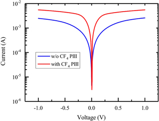
As an application test we characterized the NiSi/p-Si (100) Schottky contacts formed with 8 nm Ni at 500 °C. Figure 9 shows the measured reverse currents of two back-to-back Schottky diodes. It is interesting that the diode on the CF4 PIII p-Si substrate shows a lower Schottky barrier height (SBH) which is indicated by the higher reverse currents. We extracted from the I–V characteristics a lower SBH of 0.410 eV on the CF4 PIII substrates compared to the SBH = 0.458 eV on Si without CF4 PIII. The improved NiSi/Si interface by CF4 PIII is reflected by the smaller ideal factor of n = 1.02 with respect to n = 1.06 for the diode on pure Si(100) substrate. The segregation of C and F atoms at the interface passivate the interface and lower the SBH. The lower SBH and n can improve the contacts for nanoelectronics.
Figure 9. I–V characteristics of two back-to-back NiSi/p-Si Schottky diodes with and without CF4 PIII before silicidation. The measured reverse currents clearly demonstrated a lower SBH on CF4 PIII Si.
Download figure:
Standard image High-resolution image
5. Conclusions
In conclusion, phase evolution of Ni silicides formed with ultra-thin Ni films on pure Si (100) and CF4 PIII treated Si (100) have been systematically studied. It is revealed that both film thickness and CF4 incorporation can affect the phase evolution and the morphology of Ni silicides. C and F atoms distributed in the silicide layer and at the silicide/Si interface decrease the interface energy, thus resulting in an increase of the critical thickness tc of direct formation of NiSi2 phase at low temperatures. With the CF4 PIII condition applied in this work tc is doubled by CF4 PIII. With a Ni layer thickness >tc, for example 8 nm Ni, CF4 PIII improves the NiSi layer uniformity and the interface smoothness. In improved layer uniformity, resistivity and SBH offer benefits for nanoelectronic applications.
Acknowledgments
The work was partially supported by National Science Foundation of China (61674161) and Open Project of State Key Laboratory of Functional Materials for Information.