

Abstract
The establishment of optical trapping theory by A Ashkin almost half a century ago led to the trapping and manipulation of micro-/nano-objects and atoms by laser beams, which is now applied in many fields. However, in a complex system where multi-physical effects interact synergistically, light–matter interaction becomes dynamic and complicated and is still poorly understood. Here, by utilising plasmonic heating, nanolithography of polystyrene (PS) films and nanomanipulation of gold nanoparticles are realised. We find that laser power and PS film thickness as well as particle shape strongly affect the etching behaviour of the PS films, which is a synergistic effect of photothermal ablation and optical forces. Theoretical calculations and simulations rationalise the proposed mechanism, which is also verified by experimental observation. This understanding not only sheds light on how the synergistic effect of photo-ablation and optical forces acts on the particles and polymer films, but also provides a guideline for light-directed single-particle-based nanolithography and nanomanipulation.
Export citation and abstract BibTeX RIS
1. Introduction
Photolithography, the most widely applied technique for nanofabrication in the information industry, suffers greatly from poor resolution due to the limit of optical diffraction, although it has advantages of high-throughput, simplicity and cost-effectiveness. Tremendous efforts have been devoted to improving the optical resolution, such as the near-field approach [1–4], the plasmonic approach [5–7] and two-photon polymerisation based on the stimulated emission depletion (STED) technique [8, 9]. However, these techniques are still based on modulation of the optics or tools/masks that are fabricated by top-down methods.
Nanoparticles, which are chemically accessible by bottom-up approaches, can be easily tailored with different sizes, shapes and compositions [10]. Due to their small size, nanoparticles are an effective nanotool for nanolithography [11]. For instance, metal-assisted chemical etching appears to be a useful technique for making Si nanostructures for photonics and electronics applications [12]. However, this etching technique is not applicable for organic polymers and cannot be directed with light to form arbitrary patterns, which significantly limits its applications. To etch polymer films, metal nanoparticles can be used as a local heating source to modify polymer films into desired surface patterns via laser irradiation [13]. By utilising their local heating effect, their etching capability can also be extended to inorganic materials with the assistance of chemical reactions [14]. In the meantime, optical forces, including the gradient force and radiation pressure (scattering and absorbance forces) may work in conjunction. However, the interplay of these multi-physical effects during laser irradiation is not well understood, especially in the case of a plasmonic nanoparticle on a substrate, the movement of which is very different from that of particles in homogeneous solutions [15–17]. This is mainly because the thermal conductivity and viscosity of the substrate can affect the resistance to the gold nanoparticles (Au NPs), which adds another layer of complexity to the system.
Although a few previous cases of utilising optical forces have shown it to be a neat technique for nanomanipulation and nanolithography, most of them are based on radial optical forces, which push the Au NPs [13, 18]. How the optical forces influence the etching of polymer films is poorly understood. Moreover, little is known about how the local temperature and viscous resistance affects the movement of Au NPs.
In this paper, we show that continuous wave (CW) laser irradiation with the presence of Au NPs not only etches polystyrene (PS) films to form subwavelength cavities but also leads to directional movement of Au NPs, which is related to the temperature and optical forces acting on the particles. Unlike the previous case where the translational stage moves during the irradiation [13] we keep the sample stationary and the particles still show directional movement although the distance moved is small (50–100 nm). The simulations and calculations further validate the proposed physical model, which is also supported by extensive experimental evidence. Although this single-particle-based etching method is not an ideal approach for high-throughput lithography, it can be an alternative tool for nanodevice fabrication and fundamental understanding. Moreover, this facile approach not only generates polymer cavities with sizes below the diffraction limit but also provides new insights on how optical forces, local temperature and the surrounding dielectric medium influence the manipulation of Au NPs.
2. Experimental section
Au NPs of size 80 nm were obtained from BBI solutions. The substrates were prepared via spin-coating of 30 mg ml−1 PS (Mw = 10 000) toluene solution on a Si substrate at a speed of 4000 rpm for 1 min. The thickness of the PS films was determined to be 120 nm via ellipsometry (α-SE). The Au NPs were drop-cast on the PS films for 10 min follow by blow drying under nitrogen gas. The samples were placed under a dark field microscope for laser irradiation. The CW lasers (532 and 635 nm) were free-space coupled to the microscope, which then focused on the Au NPs through a ×100 objective (NA = 0.8). The power of the laser was varied from 1 to 4 mW and the duration of irradiation was tuned from 5 to 360 s. Dark field spectroscopy was recorded confocally through an optical fibre (50 μm) connected to a spectrometer (QEPro, Ocean Optics). SEM images were captured with Zeiss SIGMA under an accelerating voltage of 5 kV. Simulations of the surface temperature and the electric near fields of Au NPs were performed with COMSOL (Multiphysics 5.3a). The refractive index of PS was 1.60 and that of Au was adopted from Johnson and Christy [24] with a maximum meshing size of 2 nm. Detailed parameter settings are given in the online supporting information.
3. Results and discussion
3.1. Nanoparticle-assisted photolithography of subwavelength cavities
To investigate the system, we drop-cast Au NPs (80 nm) on PS films (120 nm)/Si substrate. The scattering spectrum of Au NPs shows a plasmonic resonance at ∼560 nm. After irradiation with a 635 nm CW laser (4 mW) for 100 s, the plasmon peak redshifts to ∼620 nm (figure 1(a)) with a yellowish scattering colour (figure 1(b)). The SEM images in figures 1(c) and (d) reveal that the Au NP develops a cavity (Φ = 120 nm) in the PS film which is much smaller than the diffraction limit of 635 nm light (480 nm). Because the refractive index of the surrounding medium increases from 1 (air) to 1.6 (PS) with Si underneath after the irradiation, it is reasonable to expect a redshift of the plasmon peak as shown in figure 1(a). However, it is not obvious why the Au NP concaves the PS film, as the maximum surface temperature (from simulation) of a Au NP when irradiating at this power (4 mW) is 460 K (figure 1(e) and figure S2 available online at stacks.iop.org/NANO/30/305304/mmedia), which is not sufficient to degrade the underlying PS films (Td = ∼550K). This etching process is not likely due to the near-field-enhanced photochemical degradation as PS does not absorb 635 nm light and no cavities are generated if the irradiated region contains no Au NPs.

Figure 1. Light-directed single Au NP (80 nm) based nanolithography of PS films: (a) scattering spectra, (b) dark field and (c), (d) SEM images of the Au NP before and after laser (635 nm) irradiation (4 mW, 100 s). Scale bars are 100 nm. Theoretical calculations of (e) surface temperature of the Au NP at different laser powers, (f) viscosity (blue line) and viscous resistance (red line) of PS at different temperatures.
Download figure:
Standard image High-resolution image3.2. The temperature and optical forces
Although the surface temperature of the Au NP is not high enough for thermal degradation of the polymers, it is sufficient to melt the PS films locally if the laser power is above 3 mW (figure 1(e)). In addition, the focused laser beam can exert radiation pressure ( ) on the Au NP, which pushes it into the PS films if the viscous resistance (Fv) is small. To rationalise this process, we use the dipole approximation to calculate the radiation pressure using the formula [19]

where  is the extinction cross-section of the Au NPs (figure S1),
  is the intensity of the laser beam, n is the refractive index of the environment and c is the speed of light. This dipole approximation is qualitatively fine in this system.
As for the calculation of the viscous resistance, Fv, of the PS films, we apply the Stokes equation [20]

where r is the radius of Au NP, v is the speed with which the Au NP moves in the molten PS film and  is the viscosity of the PS, which is dependent on temperature (blue line in figure 1(f)) [21].
For 4 mW laser irradiation, the calculated results (see the online supporting information for detailed calculations) show that the radiation pressure acting on the Au NP gradually increases from 0.2 pN to 1.6 pN (figures 2(a) and (b)) when it enters into the PS film, which is sufficient to overcome the viscous resistance (0.1 pN) at this temperature (red line in figure 1(f)). Therefore, it is plausible that the Au NP can be pushed into the PS film by radiation pressure even if we ignore the gravitational force on the Au NP.
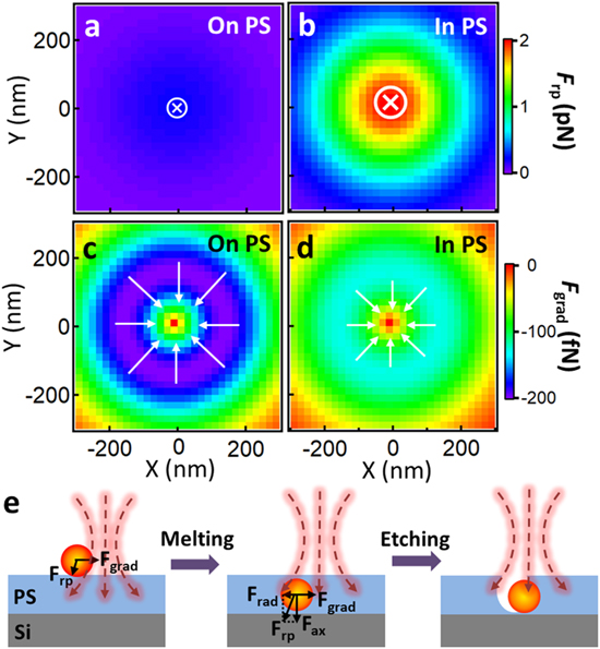
Figure 2. Theoretical calculations of (a), (b) radiation pressure and (c), (d) gradient force experienced by a Au NP on PS (a), (c) and in PS (b), (d). The irradiance beam power is 4 mW with waist size of 300 nm. (e) Proposed anisotropic etching mechanism of PS film with a Au NP irradiated by 635 nm laser beam.
Download figure:
Standard image High-resolution imageWhat is intriguing, however, is that the Au NPs appear to deviate from the centre of the cavities, which is independent of polarisation (figures 1(d) and S4). Such deviation is proportional to the irradiation time with distance up to 50 nm (figure S5). Thus, this deviation is not likely to be due to microscope stage vibration or drifting as these artifacts will only result in much larger deviation without any trend. We interpret that some forces push on the Au NPs horizontally so that they stick to the walls of the cavities rather than staying at the bottom. The possible forces that may take effect in this scenario are optical forces and photophoretic forces, which are commonly observed in plasmonic systems and have been applied to manipulate micron-sized particles [22]. Photophoretic forces, which arise from the thermal gradient within the particle, are negligible in this case as the Au NP (80 nm) is much smaller than the laser beam spot size. Therefore, the main contribution of the forces that move the Au NPs seems to be the radial component of radiation pressure ( ) and optical gradient force (
 ), which can be calculated using the formulae [23]


where  is the angle between the axial component of radiation pressure (
 ) and
) and  ,
,  is the polarizability of Au NPs, z is the wave impedance in a vacuum and
  is the intensity gradient. These two forces are opposite to each other but because
  (∼0.1–0.2 pN) is slightly larger than
  (∼0.02–0.14 pN) (figures 2(c), (d)), the net force direction on the particle is towards the beam centre. As a result, the Au NP is pulled to the beam centre when it develops a cavity in the PS film, leading to anisotropic etching (figure 2(e)).
During the optical pushing, the surface temperature of the Au NP increases up to 569 K (figure 3), which is due to the increased intensity of the electric near field as the Au NP moves into the PS film (figure S3). As a result, it starts to degrade the PS at the stage when it is fully embedded, causing a cavity to form around the Au NP. The temperature drops dramatically to 330 K if the Au NP touches the Si substrate (figure 3(e)), which is due to the good thermal conductivity of Si (∼150 W K–1 m–1). Therefore, it is likely that a thin layer of PS exists between the bottom of the cavities and the Si substrate as the lowered temperature of the surrounding PS significantly increases the resistance against the Au NPs, which stops them from moving downwards. Therefore, the distance moved by Au NPs in PS films, besides the magnitude of optical forces, is also dictated by the thickness of the PS film.

Figure 3. Simulations of the surface temperature of Au NPs at different PS film depths: (a) on the PS film surface, (b) 20 nm, (c) 40 nm, (d) 60 nm and (e) 80 nm below the surface of the PS film. All the scale bars are 200 nm. (f) Summary of the variation of Au NP surface temperature with the height of Au NPs above the Si substrate. (Note that the surface of the Si substrate is defined as zero). The light blue region denotes the decomposition zone (De-zone) and the pink region denotes the viscous flow zone (Fl-zone).
Download figure:
Standard image High-resolution imageTo verify this, we used a 532 nm laser for the particle irradiation, which is close to the plasmon resonance (red line in figure 1(a)). Thus, this optical heating is more prominent, which increases the temperature of Au NPs up to 566 K with only 1 mW power (figure S6). However, due to the cooling effect of the Si substrate, as mentioned above, the Au NPs only travel a limited length of ∼50 nm for a thin PS film (120 nm), irrespective of the irradiation time and irradiation wavelength (figures 1(d) and 4(a), (b)). If the thickness of the PS film is increased to 200 nm, the Au NP travels with much larger distance (up to ∼300 nm), and embeds itself into the PS film (figure 4(c)). As such, the distance that the Au NPs travel is determined by the PS film thickness due to the cooling effect of the substrate (figure 4(d)).

Figure 4. Irradiation of a Au NP on a PS/Si substrate (532 nm CW laser, power 1 mW). In (a) and (b) the PS film thickness is 120 nm; irradiation time (a) 20 s and (b) 60 s. In (c) the PS film thickness is 200 nm and the irradiation time is 20 s. (d) Scheme of Au NP track etching in PS films of different thicknesses.
Download figure:
Standard image High-resolution image3.3. The etching conditions
Based on the etching mechanism mentioned above, the formation of cavities in PS films is affected by irradiation time, laser power, wavelength and the shape of Au NPs as these factors influence how much heat is generated around a Au NP. For a 4 mW CW laser (635 nm), the irradiation time needs to be above 60 s to clearly observe a cavity around the Au NP (figure 5(a)). However, if a 3 mW laser is applied, a longer irradiation time (100 s) is required for clear cavity formation (figures 5(b), (c)). A 2 mW laser does not seem to be capable of generating cavities for the irradiation time we have applied (figure 5(d)) as the temperature is below the viscous flow temperature of PS (figure 1(e)). The etching diagram of irradiation conditions (figure 5(h)) suggests there is a certain threshold of time and power above which nanoparticle-assisted photolithography can occur. Moreover, using Au NPs with a smaller size (60 nm) also makes etching of PS films difficult even after irradiation for 120 s (figure 5(e)). This is mainly because of the lowered surface temperature of Au NPs with smaller absorbance cross-section. But for a Au prism with the same effective diameter (∼60 nm), etching can be observed (figure 5(g)) (4 mW, 120 s) as the field is more concentrated around the corners, which produces a much larger absorbance cross-section than with its spherical counterpart, leading to a higher surface temperature for thermal degradation. The size of the particle used for etching can be even smaller as long as it produces sufficient heat for photothermal degradation. But it will be challenging to locate the particles less than 50 nm under dark field optical microscope. All of this evidence again suggests that it is the plasmon-assisted photothermal effect that degrades the polymers locally, forming the concave etching.

Figure 5. SEM images of irradiated Au NPs in/on PS films at different conditions: 635 nm laser irradiation for 60 s and laser power of 4 mW (a) or 3 mW (b); irradiation for 100 s with a laser power 3 mW (c) or 2 mW (d). Irradiation of Au NPs (4 mW for 120 s) with different sizes and shapes: (e) 60 nm Au nanosphere, (f) 80 nm Au nanosphere, (g) 60 nm Au nanoprism. (h) Etching diagram for 80 nm Au NPs irradiated at different conditions.
Download figure:
Standard image High-resolution imageAs the shape of the nanoparticle determines the shape of the cavity, we can engineer the shape of the cavity by using different shaped plasmonic nanoparticles and their assemblies. For instance, ellipsoidal cavities can be formed either with a Au NR (figures 6(a), (b)) or Au dimer (figures 6(d)–(f)) as the heating particles. The aspect ratio of the cavity can be increased by using a Au NR dimer as the heating nanoparticle (figure 6(c)). These Au NPs can be removed by wet etching, leaving an empty hole in the PS film (figure S7). As such, the combination of differently shaped NPs and their assemblies significantly enriches the etching morphology of the cavities, making it tailorable for different applications.

Figure 6. SEM images of nanoparticle-assisted photothermal etching of non-spherical cavities using non-spherical particles. (a), (b) Au NR and (c)–(f) Au dimer before (a), (d) and after (b), (c), (e), (f) laser irradiation (4 mW): (b) Au NR 100 s, (c) Au NR dimer 180 s, (e) Au dimer 100 s, (f) Au dimer 180 s.
Download figure:
Standard image High-resolution image
4. Conclusions
In summary, light-directed subwavelength etching of PS films is realised with the assistance of plasmonic NPs, and generates cavities via near-field photothermal ablation. The Au NPs appear to deviate from the cavity centre, which is due to optical forces. We summarise this anisotropic etching mechanism as optical-force-assisted photothermal lithography. The Au NPs under laser irradiation generate sufficient heat to melt the PS films underneath. The radiation pressure from the focused Gaussian beam pushes the Au NPs into the PS films, which further raises their surface temperature above the degradation temperature. This degradation significantly reduces the resistance to horizontal movement invoked by the gradient force. As a result, the Au NP starts to move towards the beam centre, resulting in anisotropic etching. The direction of movement of the Au NPs is rather random (figure S4) as the placement of Au NPs within the Gaussian beam is not well-controlled due to optical diffraction. These proposed mechanisms are validated with both experimental evidence and theoretical calculations. This work not only reveals the complicated interplay of optical forces and photothermal effects on Au NPs, but also provides a facile route for subwavelength lithography, particle manipulation and plasmon fine-tuning.
Acknowledgments
This research is supported by the NSFC (21703160), the Fundamental Research Funds for the Central Universities (2042018kf0254, 2042018kf0038). We thank the Supercomputing Center of Wuhan University for the support of numerical calculations in this paper.