

Abstract
I–VI chalcogenide low-toxicity semiconductors and their near-infrared optical property are of great importance for solar cell and biological probe applications. Here, we report the synthesis of Ag2SxSe1−x (x = 0–1) ternary nanocrystals (NCs) and their photoelectrochemical properties, using a refined simple hot-injection reaction recipe. The ICP-MS results show the change of non-metallic composition in products and precursors, which can be well fitted with Vegard's equation. Ternary alloying broadens the absorption spectrum region of Ag2S NCs. It can also balance the transfer of photo-excited electrons through the interfaces of TiO2/Ag2SxSe1−x and Ag2SxSe1−x/electrolyte by minimizing electron–hole recombination. By tuning the compositions, an increase in power conversion efficiency (PCE) was observed with the increase of S composition and the size of the NCs. The photoelectrochemical results reveal that Ag2SxSe1−x ternary NCs exhibit higher conversion efficiency than pure binary NCs. The drop in PCE of the binary NCs is mainly attributed to the decreases of the charge separation following exciton transition.
Export citation and abstract BibTeX RIS
1. Introduction
Infrared materials are of great importance in solar cell, detector and biological probe applications, because the infrared light (beyond 700 nm) occupies about 70% photon flux of the whole sun light energy and it can penetrate deep tissues without the influence of bioluminescence. Previous works about infrared materials are mainly concentrated on CdTe [1, 2], InAs [3, 4], PbS and PbSe [5–10] nanocrystals (NCs) and their variations [11, 12]. However, the intrinsic toxicity of these materials restricts their applications. Thus, it is urgent to find environmentally friendly materials [13]. I–VI semiconductor NCs (Ag2X, X = S, Se, Te), as typical near infrared (NIR) materials, have some unique properties such as low toxic [14–16], high ionic and electronic mobility [17], and high electrical conductivity [18, 19]. Ag2X NCs provide a broadband absorption in the NIR region, which is an intrinsic advantage to improve the efficiency of the photovoltaic devices. Although there are quite a few reports about photovoltaic device structures, they performed poor power conversion efficiencies (PCEs) [20–25].
Compared with binary NCs, ternary alloyed NCs have some superior properties. For example, bandgap tuning is crucial in photovoltaic devices. With the composition control of ternary alloyed NCs, one can obtain different bandgap materials without changing the particle size [26–28]. Alivisatos' group reported PbSxSe1−x NC photovoltaic devices and the results showed that the ternary alloys were more efficient than pure binary alloy NCs based devices [29–31]. Zhong and coworkers described CdSexTe1−x alloyed NCs sensitized solar cells with greater than 6% efficiency and high stability [32]. Moreover, ternary alloys supply a unique way to investigate the micro interaction of exciton and hole or other electron−hole decoupling [33, 34].
In this work, monodisperse Ag2SxSe1−x ternary NCs with successive size tunability were synthesized using a modified synthesis method. Different ratios of high reactivity precursors (TMS)2S and (TMS)2Se were used to adjust the band-gap of the NCs. High reactivity precursors can overcome the intrinsic lattice mismatch that play important roles in crystal growth orientation and final morphology. Furthermore, the photoelectrochemical performance, as an evaluation index, shows that composition doping bring about an impressive promotion to photocurrent. Benefited from composition regulation, we obtained different band-gap materials without size change, which is of great importance to the photovoltaic devices.
2. Experimental section
2.1. Materials
Bis(trimethylsilyl)sulfide ((TMS)2S, 98%, Sigma Aldrich), bis(trimethylsily)selenide ((TMS)2Se, 98%, Sigma Aldrich), silver acetate (AgAc, 99.99%, Alfa Aesar), myristic acid (MA, 98%, J&K Scientific), octylamine (OAm, 99%, J&K Scientific), trioctylphosphine (TOP, 90%, Sigma Aldrich), 1-octadecene (ODE, 90%, Sigma Aldrich), 20 nm and 400 nm TiO2 nanoparticles (≥99.8%,Veking), titanium butoxide (98%, Sinopharm Chemical Reagent Co. Ltd), 1,2-ethanedithiol (EDT, 98 + %, Alfa Aesar), Zn(NO3)2, Na2S, hexane, methanol, toluene, and acetone were used as received.
2.2. Preparation of (TMS)2S-TOP and (TMS)2Se–TOP precursors
The precursors of (TMS)2S–TOP and (TMS)2Se–TOP were prepared in a glove box. The total number of moles of S and Se was kept at 0.40 mmol and the two precursors with different atomic ratios (S/(S + Se) = 0, 0.25, 0.5, 0.75, 1) were mixed with 10 ml TOP in a glass vial with vigorous stirring, then the precursor solution was transferred into a 20 ml syringe.
2.3. Synthesis of Ag2SxSe1−x NCs
We modified the synthesis route of Ag2SxSe1−x NCs based on a method reported by Pang et al [35]. The synthetic process was performed by adding 0.4 mmol AgAc powder, 6.4 mmol MA, 9.6 mmol OAm and 25 ml ODE in a 100 ml three-neck flask under continuous stirring. Then the solution was degased by vacuum for at least 1 h. After this procedure, the system was protected by N2 atmosphere throughout the reaction. Followed the purging progress, the solution was heated to 80 °C for 5 min, and 5 ml OAm was injected. When the AgAc powder completely dissolved, the solution turned to be transparent. The reaction system was then cooled down to 50 °C, and the (TMS)2S–TOP and (TMS)2Se–TOP mixture was injected into the flask swiftly. After the injection, the temperature was adjusted to 40 °C, the color of the solution immediately changed from transparent to dark, indicating the formation of the NCs. The temperature of the reaction system was set at 40 ± 0.3 °C for 5 min to guarantee the stable growth of the NCs.
2.4. Purification of Ag2SxSe1−x NCs
The reaction was quenched by injecting 10 ml 4 °C anhydrous toluene and immersing the flask into an ice-water bath. The as synthesized NCs were purified by adding 25 ml of anhydrous methanol/acetone to make the NCs precipitate out and then centrifuged at 6000 r min−1 for 20 min This step was repeated at least three times. The gained brown-black product was dissolved in 5 ml hexane and centrifuged again at 12 000 r min−1 for 3 min to remove any big size of impurity. At last, the pure product was filtered by a 0.22 μm filter and transferred into a glove box for further use.
2.5. Characterizations
The microstructures of the samples were measured by using field emission scanning electron microscopy (FESEM, JEOL JSM-6700). A JEM 2100 F was used to measure the transmission electron microscopy (TEM) and high resolution transmission electron microscopy (HRTEM). The acceleration voltage was 200 kV. The samples of TEM were made by dropping the NCs (dissolved in hexane) onto carbon film coated copper grids and let it dry. The absorption and photoluminescence spectra were recorded by Shimadzu UV-3600 spectrophotometer and Omni-λ300 monochromotor/spectrograph, respectively. X-ray diffraction (XRD) patterns were obtained using a Bruker D8 Advance XPert diffractometer (Cu Kα: λ = 1.5406 Å), in the range of 10°–70° at a scan rate of 4 ° min−1. Inductively coupled plasma mass spectrometry (ICP-MS) was performed on Agilent/7700. X-ray photoelectron spectroscopy (XPS) was conducted on an ESCALAB250 spectrometer. The highest occupied molecular orbital (HOMO) energy level was measured by using high resolution ultraviolet photoelectron spectroscopy (PREVAC XPS/UPS System, R3000/VUV5K/MX-650). The film thickness was measured by Profile-system (DEKTAK 150, Vecco). Each cycle of NC film consists of successive immersion of the clean glass in NC solution for 1 min and washing with 1,2-ethanedithiol (EDT) between each step. Ten cycles were applied and the thickness was measured to be about 100 nm, so the thickness of a single layer film was about 10 nm.
2.6. Photoanode fabrication
FTO glass (Nippon Sheet Glass, Japan, resistance 14 Ω/square, transmittance >90% from 400 to 700 nm) was cleaned using aqueous soap solution, deionized water, ethanol and acetone for 30 min, and finally immerged into ethanol for use. TiO2 nanorods (NRs) were grown on FTO glass by a hydrothermal method reported in the literature [36]. Briefly, 60 ml concentrated hydrochloric acid (36.5%–36.8% by weight) was added to 60 ml double-distilled water under vigorous stirring for 5 min, then 1.2 ml titanium butoxide was added to the mixture. After continous stirring, 30 ml of the mixture was transferred into a 100 ml Teflon-lined stainless steel autoclave. Three pieces of FTO glass were placed against the wall of the Teflon-liner with a slope. After treated with hydrothermal method at 180 °C for 14 h, the FTO glass was rinsed with double-distilled water and ethanol, and immersed into 50 mM TiCl4 aqueous solution for 30 min at a 50 °C water bath. The TiCl4-treated sample was annealed at 500 °C for 2 h. Two layers (an active layer and a scattering layer) of TiO2 nanoparticles (NPs) were then modified onto FTO/TiO2 NRs. The TiO2 paste (particle size ∼20 nm) was applied onto the FTO/TiO2 NRs as an active layer by a blade. The film was dried in a muffle furnace at 80 °C for 1 h and followed by annealing at 500 °C for 2 h. The scattering TiO2 layer (particle size ∼400 nm) was coated onto the active layer by a blade, then the electrode was dried in the muffle furnace at 80 °C for 1 h and annealed at 500 °C for 2 h.
2.7. Electrophoretic deposition (EPD)
EPD was employed to fabricate FTO/TiO2 with Ag2SxSe1−x in toluene [37]. A FTO/TiO2 photoanode and a graphene electrode were placed in an electrochemical cell with a distance of 4 mm, then 150 V cm−1 bias was used to supply a constant voltage. The thickness of the NC layer could be adjusted by the EPD time and the NC concentration. After the modification, the electrode was rinsed with ethanol and dried in N2 flow.
After the EPD, we used the successive ionic layer adsorption and reaction method to coat the FTO/TiO2/Ag2SxSe1−x with a ZnS layer. Briefly, the FTO/TiO2/Ag2SxSe1−x photoanode was dipped into cationic sources (Zn(NO3)2 solution, 0.1 M in methanol) and anionic sources (Na2S solution, 0.1 M in Vmethanol:Vwater = 1:1) for 1 min, respectively. This process was repeated for two cycles. Between each cycles, the photoanode was rinsed with deionized water.
2.8. Photoelectrochemical measurements
Photoelectrochemical measurements were performed in a quartz cell (20 mm × 20 mm) containing a sulfide/polysulfide electrolyte ( 0.25 M Na2S and 0.35 M Na2SO3 dissolved in deionized water). FTO/TiO2/Ag2SxSe1−x, Ag/AgCl (3 M KCl), and Pt foil electrode were employed as the photoanode, reference and photocathode, respectively. The photovoltaic performances of photoelectrochemical cells were evaluated using an electrochemical workstation (Corrtest CS150). An AM 1.5 light with a power of 100 mW cm−2 (from Zolix SS150 solar simulator) was employed as the illumination source. The efficiency of the light source at different wavelengths was measured using (Newport) QE/IPCE measurement kit with a silicon detector.
3. Results and discussion
It is not easy to achieve monodisperse ternary NCs because many factors will influence the result in microscopic scale, such as the reactivity of passivation group, the temperature, and the concentration of precursors. Among these factors, the relative reactivity of two competitive precursors (S and Se in this case) is of great importance [26]. Precursors with different activities will lead to separated nucleation. So it is hard to obtain ternary alloyed NCs and the size homogeneity of the NCs usually deteriorates. Take this factor into consideration, one should choose the precursors with comparable reactivity to reduce the individual self-nucleation, and adjust the molar ratio of both precursors to make the desired composition in the NCs. S powder and Se powder dissolved in trioctylphosphine (TOP) were firstly selected as the precursors. The TEM images displayed bad size distribution, and serious self-nucleation of Ag2S and Ag2Se. (TMS)2S and (TMS)2Se were finally selected as the ideal precursors. Because trimethylsilyl terminated S and Se atoms have high and comparable reactivity, which would ensure the homogeneous nucleation of ternary NCs at low temperature. Figure 1 exhibits the TEM and element mapping images. To gain strong element signals, we exchanged the myristic acid and octylamine ligands to butylamine and washed the NCs more than 30 min The nucleation was a fast step in a few seconds, with growth step carrying on; the comparable reactivity of two precursors made them react in a similar ratio of feeding atoms. Finally, we gained nearly uniform sized NCs as shown in figure 1 with good crystallinity. Figure 1(a) is the TEM image of Ag2S0.66Se0.34 NCs, and the white frame zone was selected to scan atom mapping image. HRTEM indicated the lattice spacing of 0.223 and 0.243 nm corresponding to the (103) and (013) planes of orthorhombic phase, respectively. The separated maps in figures (b)–(d), illuminate that Ag, S and Se were distributed evenly in the NCs.
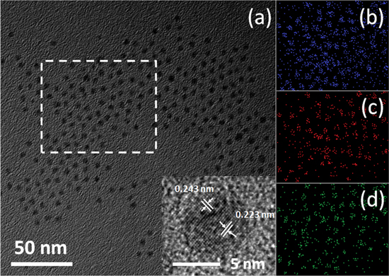
Figure 1. (a) TEM image and HRTEM (inset) of Ag2SxSe1−x NCs. Element maps of (b) Ag, (c) Se and (d) S in blue, red and green, respectively.
Download figure:
Standard image High-resolution imageICP-MS was applied to analyze the actual atomic ratio of S and Se anions in the product. 3 ml aqua regia was used to dissolve 6 mg samples and then diluted by 25 ml deionized water. The result in figure 2(a) is the proportion of S atom (S/(S + Se)) in precursors and products collected from 9 samples. When the molar ratio of the precursor was set at 1:1, the S and Se found in the product was close to 1:1 (i.e., Ag2S0.48Se0.52). It is attributed to the comparable reactivity of Se precursor and S precursor that the graph shows a better linearity than the previous reported result [31]. The S element analysis in figure 2(b) demonstrates the trend of S composition varied a little in the beginning of the reaction, and quickly reached a steady level of (S/(S + Se)) ≈ 0.5.

Figure 2. (a) ICP-MS data show the relative amount of S in the product versus the relative amount of S in the precursor solution. (b) S element in NCs taken from products reacted for 0–30 min.
Download figure:
Standard image High-resolution imageThe absorbance and photoluminescence spectra of Ag2SxSe1−x NCs are shown in figures 3(a) and (b) with a strong excitonic absorption peak. The photoluminescence peak positions are located at 1026 nm, 933 nm and 847 nm for Ag2Se, Ag2S0.48Se0.52 and Ag2S NCs. The calculated Stokes shift is around 180 nm for the three NCs. The spectrum shifted to red with the increase of Se composition. As Vegard's law [38] says, this shift of alloyed materials can be described as Ealloy = χEA + (1 − χ)EB, where χ is the molar fraction of component A, EA, EB, and Ealloy are the band gap energies (or other physic properties) of pure A, pure B, and the alloyed material, respectively. Figures 3(a) and (b) reveal that both of the photoluminescence and absorption spectra follow the Vegard's law. Fortunately, the precursors' high reactivity ensures the smooth growth of the ternary NCs even at low temperature, thus we did not observe an 'optical bowing' effect as reported in CdSexTe1−x alloys synthesis [39].
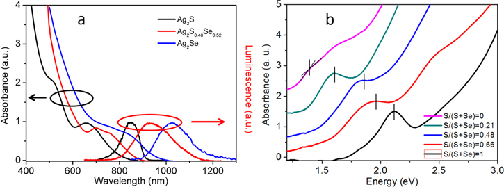
Figure 3. (a) Absorbance and photoluminescence of Ag2Se, Ag2S, and Ag2S0.48Se0.52. (b) Absorbance spectra of alloyed NCs with gradient varied ratio of S and Se in precursors.
Download figure:
Standard image High-resolution imagePhase identification of Ag2S, Ag2S0.48Se0.52, and Ag2Se NCs in figure 4 were carried out by XRD measurement. The XRD patterns show that monoclinic Ag2S formed in our synthesis and all the characteristic diffraction peaks can match the JCPDS card very well (JCPDS, 14-0072). The lattice fringe of Ag2S (−013) with spacing of 0.238 nm is a dominant orientation which is also observed in figure 6. The diffraction peaks of Ag2Se NCs correspond to the orthorhombic Ag2Se in the β form (JCPDS, 24-1041). The lattice fringe of Ag2Se (121) is corresponding to the fringe spacings of 0.258 nm in figure 6. The characteristic peaks of Ag2S0.48Se0.52 NCs appear between the two pure materials (JCPDS, 27-0620), which is a gradient chang between Ag2Se and Ag2S NCs. Two dominant orientations of Ag2S0.48Se0.52 (013) and Ag2S0.48Se0.52 (103) with fringe spacings of 0.243 and 0.223 nm are also observed in figure 6. The broadenings of the peaks of NCs disclosed the nanocrystalline nature of the products, which primarily related to the size of NCs which are much smaller than their bulk materials.
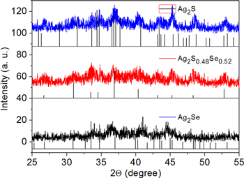
Figure 4. XRD plots of Ag2S, Ag2S0.48Se0.52 and Ag2Se NCs.
Download figure:
Standard image High-resolution imageXPS was measured to investigate the surface composition and valence condition of the NCs. Figure 5(a) is the low-resolution scan spectrum of Ag2S0.48Se0.52 NCs. Figures 5(b)–(d) are the high-resolution scan spectra of the Ag 3d, S 2p, Se 3p, and Se 3d. The binding energy of Ag (3d3/2, 5/2) emerges at 373.60 and 367.60 eV, respectively, suggesting that the oxidation state of silver is univalent Ag+ in the NCs [40]. As for Se element, the peak of Se (3d3/2, 5/2) is observed at 53.51 eV. Because the peaks of S and Se elements have an overlap, it is essential to separate them by a fitting method. After fitting, Se 3p1/2 and Se 3p3/2 appear at 159.32 and 165.33 eV, respectively. So the resolved signals eliminate the existing of mutiple oxidation states of selenium within the peak range. In other words, the valence of selenide is Se2− [41, 42]. S 2 P appears at 160.45 and 161.32 eV based on the possible peak fitting result, which demonstrates the existing of S2−. All the experiment data are consistent with the previous reports [41, 43].

Figure 5. XPS spectra (a) show the present of Ag, S and Se elements. High resolution XPS spectra for Ag 3d (b), S 2p (c), Se 3p (c), and Se 3d (d) show the surface valence condition of the Ag2SxSe1−x NCs, (c) The overlapped spectra of Se and S were fitted with gauss method.
Download figure:
Standard image High-resolution imageThe TEM and HRTEM images in figure 6 show the shape, structure, and size of the NCs. The size distributions of the NCs were nearly monodisperse. The sizes of the spherical NCs were 5.2, 6.8 and 9.2 nm, respectively. With the ratio of S/(S + Se) decreased, the lattice spacing changed from 0.238 to 0.243 and finally to 0.258 nm. The same trend was also observed from XRD results in figure 4. The uniform lattice structures and nanocrystal sizes demonstrate that there is no core/shell structure or stack faults. In other words, S and Se atoms grew within the ternary NCs.

Figure 6. The typical TEM images of Ag2S (∼5.2 nm) (a), Ag2S0.48Se0.52 (∼6.8 nm) (b), and Ag2Se (∼9.2 nm) (c) NCs. The insets are the HRTEM images, which show clear lattices of the NCs.
Download figure:
Standard image High-resolution imageThe SEM images in figure 7(a) reveal that the FTO surface covered with compact TiO2 crystal seeds. TiO2 NRs grow above the seeds uniformly. The length of TiO2 NR is about 1 μm and the diameter is between 80 and 120 nm, respectively. The planar density is about 8–12 wire μm–2. Figure 7(a) gives the tilted cross view of the TiO2 NRs treated with TiCl4. In the image, we can observe that the TiO2 NRs covered densely, uniformly and nearly vertical on the FTO substrate. The quadrangular prism morphology reveals that the TiO2 NRs are tetragonal crystal structure. After being treated with TiCl4, TiO2 NCs with diameter ∼5 nm grow onto the surface of TiO2 NRs. This procedure effectively enhances the specific surface area of NRs, which helps the large scale coating of Ag2SxSe1−x NCs onto the TiO2 NRs surface. Figures 7(b) and (c) demonstrate that Ag2SxSe1−x NCs were deposited on the TiO2 NRs. After the deposition process, the space between the NRs was compactly covered with Ag2SxSe1−x NCs. The rough surface of the NRs became even rougher after overgrown with Ag2SxSe1−x NCs. The HRTEM in figure 6(d) show the interface of the TiO2 NRs and Ag2SxSe1−x can be clearly distinguished for a high crystallinity. The lattice fringes of rutile TiO2 (101) and Ag2S0.66Se0.34 (013) with spacings of 0.246 and 0.243 nm are denoted in the figure 7(d). The approximate lattice parameter can ensure the stable growth of two crystals from dynamic aspect.
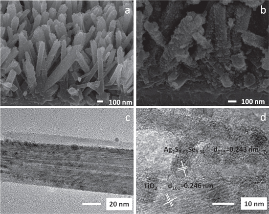
Figure 7. (a) SEM images of TiCl4 treated TiO2 NRs. After the treatment, TiO2 nanoparticles grow at the surface of the TiO2 NRs, which can increase the surface area of the NRs. (b) FTO/TiO2/Ag2SxSe1−x photoanode exhibits large amount of Ag2SxSe1−x NCs after the electrophoretic deposition compared to TiO2 NRs. (c) Low-magnification TEM image shows the uniform morphology of TiO2/Ag2SxSe1−x. (d) HRTEM image shows the interface and crystalline structure of the TiO2/Ag2SxSe1−x.
Download figure:
Standard image High-resolution imageUPS was used to measure the kinetic energy of Ag2SxSe1−x NCs. The NCs were coated on a piece of clean glass and the film thickness was controlled to be 10 nm. Figure 8 shows the Fermi energy levels. The peak absorption values taken from figure 3 are used as the band-gap (2.12 eV for Ag2S, 1.97 eV for Ag2S0.66Se0.34, 1.85 eV for Ag2S0.48Se0.52, 1.61 eV for Ag2S0.21Se0.79 and 1.39 eV for Ag2Se). We calculated the HOMO and lowest unoccupied molecular orbital (LUMO) energies of Ag2SxSe1−x NCs. Here, Ag2SxSe1−x NC photoelectrochemical cells are N type solar cell structure. The LUMO energy level of NCs must higher than the LUMO energy level of TiO2 NRs. Based on the precise energy level positions, we could design the structure of photoelectrochemical cell more reasonably. The LUMO and HOMO energy levels were −3.47 and −5.60 eV for Ag2S, −3.49 and −5.46 eV for Ag2S0.66Se0.34, −3.43 and −5.28 eV for Ag2S0.48Se0.52, −3.45 and −5.06 eV for Ag2S0.21Se0.79, and −3.44 and −4.84 eV for Ag2Se, respectively.

Figure 8. UPS data of Ag2S, Ag2S0.66Se0.34, Ag2S0.48Se0.52, Ag2S0.21Se0.79 and Ag2Se NCs. The left panel shows the amplified views of the high binding energy regions and the right panel displays the amplified views of the low binding energy regions.
Download figure:
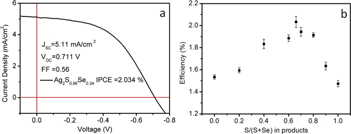
Standard image High-resolution imageFinally, we tested the photoelectrochemical cell performance using Ag2SxSe1−x NCs with different ratios of S and Se. Figure 9(a) shows that the Ag2S0.66Se0.34 NCs have an excellent performance of 2.034% IPCE due to its highest photocurrent in figure S1(b) (supporting information), and ternary alloy NCs give higher PCEs than binary NCs in figure 9(b). The interpretation is that ternary alloy can broaden the absorption spectrum region of Ag2S NCs and the photocurrent will be higher with the increase of photogeneration carrier concentration. At the same time, ternary alloy can balance the transfer of photo-excited electrons through both interfaces of the TiO2/Ag2SxSe1−x and the Ag2SxSe1−x/electrolyte by minimizing electron–hole recombination. When the composition of Se increased, the band-gaps of the ternary alloy NCs decreased. The obtained highest photocurrent value is 5.11 mA cm−2. With further increase of Se composition, we observed a decrease in photocurrent due to the electron–hole recombination in figure S1(b) (supporting information). Taking the absorption factor into consideration, we prolonged the reaction time of the NCs to gain relative bigger NCs, which is a good way to promote the photon absorption. During the composition adjusting process, the LUMO energy level stayed steady with the gradual variation of S and Se composition (figure 8), which is consistent with the variation trend of open voltage in figure S1(a) (supporting information). Benefited from the use of composition hybridization and bis(trimethylsilyl) group, the surface passivation ligand is stable to the ambient atmosphere and electrolyte solution. The interpretations is that the morphology change decreased the aggregation of the NCs [44]. It can also supply a stable photocurrent under continuous work in figure S2 (supporting information). On the basis of these results, composition adjustment helps us find the optimal value of ternary NCs that supplies the highest PCE. Alloying has been proved to be a simple and useful method to achieve target band-gap and maintain the binary advantages.
Figure 9. (a) J–V curve of Ag2S0.66Se0.34 NCs under AM 1.5 irradiation. (b) Photoelectrochemical cell performance with different S/(S + Se) ratios.
Download figure:
Standard image High-resolution image
4. Conclusion
In summary, we have synthesized and characterized monodispersed Ag2SxSe1−x NCs. HRTEM and XRD confirmed the lattice change; the lattice parameter gradually shifted from Ag2S to Ag2SxSe1−x and finally to Ag2Se NCs. The HOMO and LUMO energies were also determined by UPS and absorption spectra for the precise design of photoelectrochemical cells. The preliminary photoelectrochemical cell study demonstrated that composition dependent of band-gap tuning of the ternary alloying helped to enhance the photocurrent and broaden the absorption spectrum region of Ag2Sx NCs. It can also balance the transfer of photo-excited electrons through both the TiO2/Ag2SxSe1−x interface and Ag2SxSe1−x/electrolyte by minimizing electron–hole recombination. This approach turned out to be an ideal strategy to design and tuning material characteristics.
Acknowledgments
This work was financially supported by the National Natural Science Foundation of China (51272084, 61306078, 61225018, 61475062, 61675086), the Jilin Province Key Fund (20140204079GX), and BORSF LA.