

Abstract
For mass production of multiscale-optical components, microstructured moulding tools are needed. Metal tools are used for hot embossing or injection moulding of microcomponents made of a thermoplastic polymer. Microstructures with extremely tight specifications, e.g. low side wall roughness and high aspect ratios are generally made by lithographic procedures such as x-ray lithography or deep proton writing. However, these processes are unsuitable for low-cost mass production. An alternative manufacturing method of moulding tools has been developed at the Karlsruhe Institute of Technology (KIT). This article describes a mould insert fabrication and a new replication process for self-centring fibre alignment structures for low loss field installable single-mode fibre connectors, developed and fabricated by the Vrije Universiteit Brussel (VUB) in collaboration with TE Connectivity. These components are to be used in fibre-to-the-home networks and support the deployment and maintenance of fibre optic links. The special feature of this particular fibre connector is a self-centring fibre alignment, achieved by means of a through hole with deflectable cantilevers acting as micro-springs. The particular challenge is the electroforming of through holes with a centre hole diameter smaller than 125 µm. The fibre connector structure is prototyped by deep proton writing in polymethylmethacrylate and used as a sacrificial part. Using joining, physical vapour deposition and electroforming technology, a negative copy of the prototyped connector is transferred into nickel to be used as a moulding tool. The benefits of this replication technique are a rapid and economical fabrication of moulding tools with high-precision microstructures and a long tool life. With these moulding tools low-cost mass production is possible. We present the manufacturing chain we have established. Each individual manufacturing step of the mould insert fabrication will be shown in this report. The process reliability and suitability for mass production was tested by hot embossing.
Export citation and abstract BibTeX RIS
1. Introduction
Microstructured metal moulding tools or mould inserts are needed for mass production of microcomponents in thermoplastic polymers or ceramic by hot embossing or injection moulding [1, 2]. Classical methods for the manufacture of moulding tools are mechanical micromachining (e.g. milling), laser machining or electrical discharge machining (EDM). Microstructured moulding tools with extremely tight specifications, e.g. in low side wall roughness and high aspect ratios are generally made by lithographic and electroforming procedures such as x-ray lithography (LIGA) [3]. The possibilities of the previously used lithographic procedures (LIGA or UV lithography) are limited. The size of the irradiation window and consequently the size of the structured surface on the tool are not arbitrarily extensible. Certain combinations of structure, dimensions and geometry of microstructures cannot be realized. At the Karlsruhe Institute of Technology (KIT), in cooperation with international partners, alternative methods in mould insert fabrication have been developed. Microstructured moulding tools are fabricated based on electroforming in nickel by galvanic replication of microcomponents. Since the early 90s the LIGA process is used as standard fabrication technology at KIT [3]. The typical LIGA process sequence starts with the generation of a polymethylmethacrylate (PMMA) microstructure or microcomponent by using LIGA. With the generated microstructures or components a mould or a mould insert is fabricated by electroforming.
Electroforming is an established mould insert fabrication technique. Before starting the electroforming process, the microstructures made from polymer are completely coated with a conductive electroplating seed layer of chrome and gold. This seed layer enables a precise metal deposition along the microstructures during electroforming. If raised structures are used, the electroforming process is carried out successfully. But if microstructures with cavities or holes are used, faults can occur during filling of the structures with nickel [4]. In this project, mould inserts are fabricated and a method is developed, which can control the electroforming process to fill holes and through holes completely with nickel. With these mould inserts, microcomponents are mass produced by hot embossing or injection moulding technologies in thermoplastic polymer [1, 2]. At KIT, the complete process chain is realized to produce high-precision moulding tools. This specifically developed equipment allows the electroforming of microstructures by transferring sacrificial polymer components into metal tools. Electroformed mould inserts provide the highest quality in structure precision, mechanical stability and durability. Thus, it would be beneficial and offering more complex geometries to use these technologies and competences also to fabricate moulding tools from other components which have been fabricated by different technologies. An example of those technologies is deep proton writing (DPW) [5].
In this paper we present the development of an alternative fabrication process for mould inserts from a microstructure component made by DPW. Different types of self-centring fibre alignment components were developed by the Vrije Universiteit Brussel (VUB), together with TE Connectivity. As method of manufacture the VUB uses the DPW as a high-precision rapid prototyping technology to generate micro-optical and micro-mechanical components based on PMMA [6, 7]. DPW finds it origins in the LIGA technology but uses protons rather than x-rays for the irradiation. As a consequence, DPW microstructures show a specific conical shape along the height due to the scattering which occurs when the impinging protons interact with the material ions. This conical shape can be of advantage for certain applications (e.g. to allow for easy fibre insertion in fibre connector structures) and—as a side effect—facilitates demoulding. The proposed mould insert fabrication scheme starts with the original component, also called the prototype or master. This can be a microcomponent or microstructure consisting of different materials, scales or functional elements. In general, microcomponents made by a lithographic technology are in polymer (e.g. PMMA). The master component for this paper is a PMMA single-mode fibre connector guide pin based alignment plate made by DPW [8]. The connector's external dimensions are 2.5 × 6.4 mm and its thickness about 500 µm (figure 1). The special feature is a three- or four-spring centre through hole in the centre of the connector. The centre hole is surrounded with slots that give the component its micro-spring functionality. On both sides of the centre hole there is a larger through hole which is used to accommodate a metal guide pin for alignment in MPO-type fibre connectors (MPO stands for multiple fibre push-on [9]). The centre hole size is slightly smaller than 125 µm and the slot holes are about 100 µm wide.
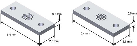
Figure 1. Design of a PMMA single-mode fibre connector with a three-spring self-centring fibre alignment structure (left) and four-spring self-centring fibre alignment structure (right) made by DPW.
Download figure:
Standard image High-resolution image2. The general technology description and experimental methods
The proposed mould insert fabrication method is mainly a combination of joining technology and electroforming (figure 2) [10, 11]. The master component is fixed on a metal substrate (e.g. copper) by adhesive bonding or mechanical clamping. In an electroforming bath the substrate and component are consequently plated with nickel. After the electroforming the nickel layer is separated of the substrate. The master component is removed from the nickel. The necessary external dimensions of the mould insert are generated by wire-cut EDM. Finally the mould insert is ready to fit into an injection moulding or hot embossing tool. As mentioned depending on the function, size and geometry of the microstructure, one of the two joining methods (adhesive bonding or mechanical clamping) is used to fix the component onto a copper substrate. This joint must withstand the electroforming process. The quality and the strength of the fixation is the key issue in this case. In addition, the joint must be free of cavities and gaps in order to prevent undesired metal deposition below the component. A copper plate represents a stable substrate and a conductive base for the electroforming process. It prevents the component from bending and deforming and supports metal deposition. The copper plate has to meet stringent requirements in terms of flatness, roughness and cleanliness, as these properties are replicated in the mould insert.
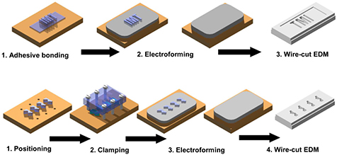
Figure 2. Schematic illustration of the alternative mould insert fabrication process steps: adhesive bonding (top) or mechanical clamping (bottom).
Download figure:
Standard image High-resolution image2.1. The adhesive bonding process
Adhesive bonding is a standard joining technology in the field of micro-system technology and a reliable low-cost joining technology. A wide range of different adhesives designed to join a huge variety of different materials are commercially available. Dispensing of adhesive from dot sizes of some few 10 µm up to larger diameters is possible. Due to the gap filling behaviour of low viscosity adhesives also delicate joining tasks can be realized. The flow behaviour of low viscosity adhesives is used to realize repeatable joints with defined forms and surfaces using surface effects like adhesion. The fixation of the polymer master onto the copper substrate is realized by adhesive bonding. A second advantage in using adhesives, in addition to the fixation, is the sealing capability. Similar to results in standard welding processes a uniform circumferential pasted seam can be built at the edge between the polymer part and the copper plate (figure 3). This meniscus is built automatically depending on different boundary conditions like the contact angle between the adhesive and the components to be joined, the viscosity of the adhesive and of course the dispensing parameters to name a few. In an optimized process, undercuts and burrs in the mould insert can be avoided and the seam facilitates demoulding from the mould insert as well.
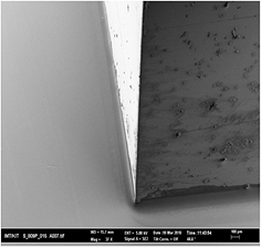
Figure 3. SEM image of an adhesive seam on the substrate along the component edges.
Download figure:
Standard image High-resolution imageFor the mould insert fabrication using micro- and nanostructured components two kinds of adhesive techniques are currently applied at KIT, which differ in the way the adhesive is prepared. In general, the dispensing technique is used [12]. For special applications and for bonding microcomponents with through holes, the dip adhesive coating method is used.
2.1.1. Dip-in adhesive bonding.
The best results in adhesive bonding with fibre connector components (containing through holes) have been achieved with the dip-in adhesive bonding or adhesive coating method (figure 4). With this method, the adhesive is not directly dispensed on the component surface. Rather first an adhesive film or layer of a defined thickness is provided and in a second step the joining surface of the component is coated by shortly dipping it into that layer. In the first process step, a special dosing device is used. This device, made of steel, offers a cavity with a predefined and precisely manufactured deepness and flat surface. The cavity is overflowed with a certain amount of adhesive depending of the cavity size. With a precise blade the adhesive is manually distributed all over the area of the cavity. During this process the polished flat rim around the cavity serves as grinding structure for the blade. After distribution a homogeneous layer of adhesive with a defined thickness is prepared. The depth of the cavity is the essential factor of this method and is essential for the desired amount and distribution of adhesive on the bonding surface of the component. In addition, other influencing effects are the viscosity of the adhesive and the wettability or the layout of the joining surface. For adhesive transfer the component with its joining surface is shortly dipped in the surface of adhesive till the complete surface is wetted and pulled out again. After the dipping, the joining surface of the component is coated with the required amount of adhesive and is placed onto the copper substrate. For the dip-in adhesive bonding of the fibre connector components, a dosing device with a cavity depth of 10 µm was used. Advantages of this adhesive application process, especially in microcomponents containing through holes, are the adjustability of the defined adhesive layer thicknesses by using different notch depths and the reproducibility of the method. Also a continuous closed seam adhesive could be created at the edges of the contact surfaces. The seam is created not only around the entire component but also simultaneously into the through holes, which prevents an uncontrolled penetration of the electrolyte during the plating process.

Figure 4. Images of a fibre connector component dip-in adhesive bonded onto a copper substrate (left), detail image of the dip-in adhesive bonded microcomponent (right).
Download figure:
Standard image High-resolution image2.1.2. Finishing treatment of adhesive bonded components by laser ablation technology.
The nickel deposition in the electroforming process cannot be carried out if the copper substrate surface is covered by an adhesive layer. When too high a dosage of adhesive has been applied, especially in micro-holes and in long and narrow trenches, the presence of an adhesive layer can inhibit an electroforming process. In a reworking step, the adhesive layer can be treated by laser technology [13]. The finishing treatment is a laser ablation process in which an excimer laser is used to remove the adhesive layer in the narrow trenches to allow a proper initiation of the electroforming process (figures 5 and 17). The laser beam is positioned over the adhesive, then penetrates into the adhesive and destroys the layer down to the copper surface. Laser cleaning was performed using a short pulse excimer laser (ATLEX-500, ATL Lasertechnik GmbH) at a wavelength of 248 nm and maximum repetition rate up to 500 Hz. The laser pulse length was 5 ns (FWHM). A homogeneous beam with a 'flat top' profile (75 µm in diameter) and an intensity fluctuation of less than 5% was established.
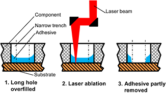
Figure 5. Schematic illustration of the adhesive removal steps by laser ablation.
Download figure:
Standard image High-resolution image2.2. The clamping process
As an alternative to adhesive bonding, the master component can be joined with the copper substrate in a force-fit manner by means of clamping. In that case the copper substrate contains tap holes. The component is positioned onto the substrate and a pressure plate is placed on top (figure 6). Usually the pressure plate is made of PMMA by micro-milling and contains micro-channels to ensure that the electrolyte can flow into all structure cavities. The plate is tightened by a screw that presses the microcomponent onto the copper plate (figure 2). Clamping is used in electroforming for about 24 h. After a nickel layer of about 200 µm has formed on the copper plate, with the microcomponent being included, the clamping plate and screws can be removed and electroforming is continued. Clamping is used when e.g. the adhesive might damage optically relevant sidewall surfaces. The clamping technology cannot be used when the component does not possess any area that is large enough to introduce the necessary pressure forces and does not permit any pressure load without deformation taking place. Further requirements on the components are sharp edges and a plane base layer. Deburred or rounded edges and an uneven basis or contact surface will result in undercuts and burrs in the mould insert. When using the clamping technique, underplating occurs more often than when using the adhesive bonding technology. Underplating is defined as an uncontrolled penetration of the electrolyte under the structure or between the copper substrate and the master. Underplating is undesirable and forms burrs at the edge of the structure in the mould insert. Finally these burrs hinder the demoulding phase in the moulding techniques (e.g. hot embossing).

Figure 6. Images of pressure plates for clamping the fibre connector (left) and a pressure plate fixed over a component and a copper substrate (right).
Download figure:
Standard image High-resolution image2.3. The electroforming and the justified partial metallization process
Before starting electroforming, master microcomponents are usually coated at KIT with a conductive electroplating seed layer of chromium and gold using a physical vapour deposition (PVD) process. This seed layer enables a precise metal deposition along the microstructures. The copper substrate with the master microcomponent is fixed to a special holder that is immersed in the galvanic bath. The galvanic system with a nickel sulfamate electrolytes containing boric acid and a flourtensid (T = 52 °C; pH 3.4–3.6) was especially developed for the electroforming of microstructures at KIT. For electroforming nickel mould inserts, the standard parameters of manufacturing mould inserts based on LIGA structures are applied [2]. Electroforming starts with a low current density (0.5 A dm−2) at the seed layer and is continued with increased current density (<1.8 A dm−2) until the metal layer has reached a thickness of 6 mm (figure 2). This leads to a stiff and homogeneous metal block which can withstand the forces applied in the moulding process.
2.3.1. Electroforming of through holes.
If there are through holes in the master, as in case of the fibre connector components used in this work, a special PVD process must be carried out. In a standard electroforming process the complete surface of the component is coated with the electroplating seed layer. Hence a nickel layer covers the complete surface of the component, sidewalls and the upper side. In case of a through hole, the nickel deposition starts inside and outside the hole at the same time. The electroplating process shows that on the edge of the hole the nickel layer grows faster than inside the hole. In this situation, the nickel layer caps the hole and inside the electroplating process is stopping. The result is a nickel mould with defects such as electroplating growth seams or voids (figures 7 and 8).
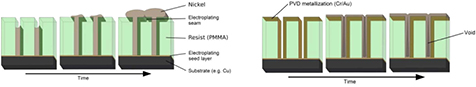
Figure 7. Illustration of the electroforming process without metallization (left) and with complete metallization (right) [14].
Download figure:
Standard image High-resolution image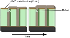
Figure 8. Illustration of the electroforming process with a partial metallization [14].
Download figure:
Standard image High-resolution imageTo optimize the nickel electroplating process for components with micro through holes a special PVD process for a justified partial metallization was developed at KIT [14]. For the electroforming process a new electroplating seed layer design was tested. This seed layer design allows guiding the formation of the electroplating nickel layer and reduces the velocity. The electroforming on the upper side does not start before the nickel has filled the complete through hole (figure 9). The new metallization design is composed of a sequence of circular spots with a diameter of 50 µm and a distance of 100 µm. The spots are created by a PVD mask and have to be adapted to the design of the master component and in particular to the position of the through holes.

Figure 9. Illustration of the electroforming process with a justified partial metallization (left) and not justified partial metallization (right) [14].
Download figure:
Standard image High-resolution image2.3.2. Fabrication of a PVD mask for the partial metallization.
First the layout of the circular spots alignment is designed using a computer-aided design (CAD) software tool. With the CAD layout a chromium mask can be fabricated (figure 10). Then in a UV-lithography process using this chromium mask, a structure with circular micro-pillars is created in a photoresist. In a nickel electroplating process the micro-pillars are surrounded with a nickel layer with a thickness of about 20 µm. Finally the resist pillars are dissolved and the PVD mask in nickel with circular holes, with a diameter of about 50 µm, is fabricated and lifted from the substrate (figure 11).

Figure 10. Schematic illustrations of the standard chromium mask fabrication steps.
Download figure:
Standard image High-resolution image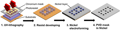
Figure 11. Schematic illustrations of the PVD nickel mask fabrication steps.
Download figure:
Standard image High-resolution imageTo use the nickel mask in a PVD process, a special holder and positioning system is needed (figure 12). It is crucial that the mask is aligned with the master component. The circular holes must be placed exactly in the right position over the component to create the electroplating seed layer spots onto the component by PVD. To meet this requirement a special holder was designed and fabricated. When using this holder the mask is clamped over the component. Under a microscope the mask is aligned by means of screws with a metric fine thread. Finally the holder, together with the mask and the component, is fixed into the PVD equipment. The results after the PVD process are exactly positioned electroplating seed layer spots on the component surface (figure 13). The microcomponent with its partial metallization layer is then ready for the electroplating process.
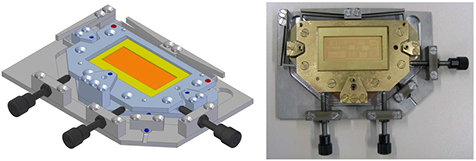
Figure 12. Images of the PVD mask holder and positioning system.
Download figure:
Standard image High-resolution image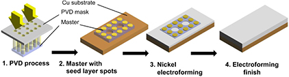
Figure 13. Schematic illustrations of the partial metallization and electroforming steps.
Download figure:
Standard image High-resolution imageThe electroplated nickel block will be separated from the substrate and processed by wire-cut EDM (figure 14).
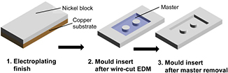
Figure 14. Schematic illustrations of the final mould insert fabrication steps after electroplating.
Download figure:
Standard image High-resolution imageDuring post-process machining, the mould insert is cut to precise exterior dimensions such that it fits into hot embossing or injection moulding tools. The current standard mould insert dimensions at KIT are 66 × 30 × 5 mm3. Once the mould insert has its final dimensions, the original component is removed from the mould insert mechanically or chemically depending on the material it is composed of. Finally the mould insert can be used for the mass production of microcomponents.
3. Results
In this work a new mould insert fabrication process was developed. The process starts with attaching the master to a copper substrate using a clamping or adhesive bonding technique, continues with the fabrication of a chromium and a PVD nickel mask and finishes with the electroplating and wire-cut EDM post-processing step (figures 10–14).
3.1. The clamping process
At the beginning of this project, the clamping technique was used to perform electroplating tests with dummy masters with the fibre connector geometry and justified partial metallization. If the results were positive, the original master components, fabricated by VUB using DPW, could be used. For these tests, dummy fibre connectors were prepared in PMMA by means of micro-milling. The mechanically prepared component was fixed onto a substrate and the PVD mask was aligned and positioned on top of it. Component and mask were installed in the vapour deposition facility and coated with the justified partial metallization (figure 13). To carry out an electroforming process, the component has been clamped after the vapour deposition process on a copper substrate, and the plating is started (figure 6). The tests of the justified partial metallization and the electroforming delivered positive results. A nickel layer with a height of 6 mm was generated (figure 15). This nickel block was separated from the copper substrate and machined to the required outside dimensions by means of wire EDM (figure 16).

Figure 15. Images of a nickel block on a copper substrate after electroforming (left) and a test mould insert after wire-cut EDM still connected with a thin copper layer (right).
Download figure:
Standard image High-resolution image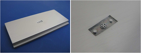
Figure 16. Images of a test mould insert after wire-cut EDM (left). The master was clamped before electroforming. The polymer master is still present in the mould insert (right).
Download figure:
Standard image High-resolution image3.2. The adhesive bonding process
After vapour deposition and electroplating tests by using the clamping technique, the gluing technique has been tested. The adhesive bonding technique tests have shown some advantages compared to the clamping technique. A particular advantage is the prevention of underplating which may occur frequently in the clamping technique. In the adhesive bonding technique, the adhesive prevents the underplating with its adhesive seam. The glue behaves like a gasket or sealing surface between the copper substrate and the component. Thus, the electrolyte cannot flow under the component and generate an uncontrolled nickel layer. A further advantage is the formation of the adhesive seam. The seam is distributed like a concave fillet weld, similar as in welding technology, both on the outer edges of the component and on the inside edges of a through hole (figure 5). This geometry generates nickel structures with rounded edges in the mould insert after electroforming (figures 17 and 18). These round edges facilitate the demoulding step in a moulding process and reduce the demoulding forces.
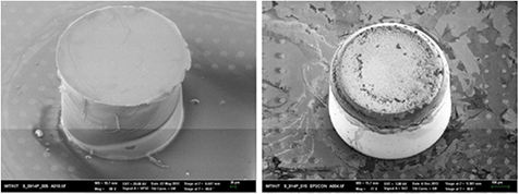
Figure 17. SEM images of electroformed pins after using the clamping process (left) and the adhesive bonding process (right). The left image clearly shows the burrs on the top edge as a result of underplating.
Download figure:
Standard image High-resolution image
Figure 18. Microscope and SEM images of the adhesive dispersion inside a long hole and a special removal detail after ablation by excimer laser (left) and the results after electroforming, rounded edges and a single pin (right).
Download figure:
Standard image High-resolution imageA further effect was observed during the adhesive bonding of the component with long and narrow trench. The narrower the trench or the higher the amount of adhesive was, the higher the risk that adhesive seams from both sides of the trench flow together and form a closed concave adhesive surface at the bottom of the trench (as shown in image 1 of figure 5). The adhesion and capillary forces increase with the amount of adhesive applied. In this case the adhesive is distributed not only on the substrate but also on the sidewalls of the long trench. Especially at the ends of the trench, adhesive piles up upwards on the sidewalls. This behaviour has the consequence, that in this area a higher adhesive seam was formed and a stronger rounded edge was generated at the nickel structure after the electroforming (figure 18). Also after the adhesive bonding technique, a nickel layer with a height of 6 mm was electroplated. The nickel layer was separated from the copper substrate and machined to the required outside dimensions by means of wire EDM (figure 19).

Figure 19. Images of a mould insert after wire-cut EDM (left). The master was adhesive bonded before electroforming. Detail image of the three-spring self-centring fibre alignment structure in the mould insert, the polymer master is already removed (right).
Download figure:
Standard image High-resolution image3.3. Justified partial metallization
The justified partial metallization was carried out successfully. The nickel PVD mask was positioned and fixed with the adjusting unit on the top of the polymer master component. The complete holder with component and mask was installed in the PVD equipment. After the vapour deposition of chromium and gold, the component was coated with the electroplating seed layer spots in the necessary areas around the holes (figure 20). The results of the partial metallization also have demonstrated that the technique is applicable for different kinds and geometry of microstructures.
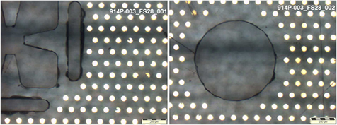
Figure 20. Images of the partial metallization, where the diameter of the spots is about 50 µm and the distance between the spots and the distance to the structure edges is about 100 µm.
Download figure:
Standard image High-resolution image3.4. Electroforming
After the justified partial metallization, the electroforming process was carried out on clamped as well as on adhesive bonded components. As required, the nickel deposition was started on the substrate surface, around the component and inside the through holes. First the nickel layer has completely filled the holes and reached the top of the component. Then the nickel layer was distributed evenly over the complete component thanks to the partial metallization (figure 21). During the electroforming process the outer nickel layer grew together with the inner layer. After an electroforming time of about 14 d, a nickel block was created with the required height of 6 mm (figure 22).
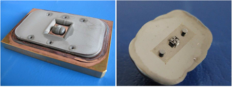
Figure 21. Images of an electroforming test with a clamped master component interrupted before the process is finished. The nickel layer has covered the copper substrate and the partial metallization (left). Detail image of the nickel deposition inside the structure cavities after the master component removal (right).
Download figure:
Standard image High-resolution image
Figure 22. Images of the complete nickel block after electroforming process with an adhesive bonded master component (left). SEM detail image of an electroformed four-spring self-centring fibre alignment structure in nickel (right).
Download figure:
Standard image High-resolution image4. Conclusions
In this work, a special manufacturing process is presented for the fabrication of nickel mould inserts for plastic-processing facilities. Using the example of a fibre connector with through holes and a self-centring fibre connector structure, the individual manufacturing steps for the fabrication of a mould insert have been carried out and are described in this report. The single-mode fibre connector, used as a sacrificial polymer component in this fabrication process, was made at the Vrije Universiteit Brussel (VUB) by DPW. At the Karlsruhe Institute of Technology (KIT) a special adhesive dip-in process was applied and a justified partial metallization technique was developed, which enabled us to successfully transfer the structure of the fibre connector into a nickel mould insert by means of electroforming. The fabricated mould insert offers the advantage of a low-cost mass production of fibre connectors made of plastic.
5. Outlook
Not only new methods were developed and tested, also new ideas were created for future applications. In particular, further work will be carried out e.g. in automation of the dip-in adhesive bonding or reducing the residual layer during the hot embossing process.
5.1. Automation of dip-in adhesive bonding
During dip-in adhesive bonding the component is coated and placed manually onto the copper substrate. In future the process sequence will be realized with the micro-assembly system NAMOSE developed by KIT in cooperation with IEF-Werner GmbH (figure 23). The NAMOSE system is based on a high-precision four-axes system with XYZ-linear movements plus Z-rotation with a workspace of 400 × 150 × 35 mm3 and a resolution of around 0.5 µm. This system offers several possibilities for tool and module fixation. The main interface at the Z-axis is based on a Schunk MWS30-system. At this interface an alignment unit for manual angular adjustment of the horizontal axes can be fixed. This unit, developed at KIT (figure 23), is used in order to adjust the parallelism of the component and the copper plate to achieve a uniform distribution of adhesive during the dip-in adhesive bonding process.
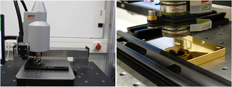
Figure 23. Images of the micro-assembly system NAMOSE (left). Detail image of the tool holder with the manual angular adjustment (right).
Download figure:
Standard image High-resolution image5.2. Optimizing of hot embossing
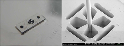
The resulting mould insert made from a DPW-fabricated PMMA master was installed in a hot embossing facility. The hot embossing system mainly consists of two separate heating plates. The mould insert is fixed onto one heating plate. Between the heating plates, a thermoplastic polymer foil is positioned, which is heated during the hot embossing step and pressed into the structures of the mould insert [1, 2]. A PMMA foil with a thickness of 1 mm was used. The mould inserts fabricated by the processes presented were tested at an embossing temperature of about 190 °C and an embossing pressure of 50 kN. In general, during hot embossing components are moulded with a residual layer (figure 24). This residual layer must be removed subsequently in one or two additional steps. In special cases and using a particular technique, hot embossing could be carried out with minimal or without residual layer [15]. After the residual-layer-free hot embossing of a fibre connector, a glass fibre was pushed into the spring-based through hole (figure 24). This paves the way towards fabrication of self-centring fibre alignment structures in large volumes.
Figure 24. Images of a moulded three-spring-design fibre connector with residual layer by hot embossing (left). SEM detail image of a PMMA four-spring self-centring fibre alignment structure moulded without residual layer by hot embossing and a glass fibre pushed through the centre (right).
Download figure:
Standard image High-resolution image
Acknowledgments
This work was supported by the Agency for Innovation by Science and Technology (IWT) under contract 095115 (EP2CON), by the FWO (Fund for Scientific Research-Flanders) under a post-doctoral research fellowship for JVE and by the Karlsruhe Nano and Micro Facility (KNMF, www.kit.edu/knmf), a Helmholtz Research Infrastructure at Karlsruhe Institute of Technology (KIT, www.kit.edu). The research has been carried out in order of TE Connectivity, 3010 Kessel-Lo, Belgium. The authors thank Marco Heiler, Paul Abaffy, Barbara Matthis, Heike Fornasier and Alexandra Moritz (KIT) for technical support.