

Abstract
Graphene-organic hybrid thin films are promising candidates for use as advanced transparent electrodes and high-performance photodetectors. In this work, we fabricated hybrid thin film structures consisting of graphene and either tetraphenyl-porphyrin (H2TPP) or metalloporphyrins such as aluminum (III) tetraphenyl-porphyrin (Al(III)TPP) and zinc tetraphenyl-porphyrin (ZnTPP). The optical and electrical characteristics of ultrathin photodetectors based on the graphene-organic hybrid layers were subsequently evaluated. A hybrid deposition system capable of both thermal evaporation and vapor phase metalation was employed to synthesize the tunable metalloporphyrin-based thin films. As a proof of concept, we successfully fabricated various graphene-based photodetectors via the simple and efficient vapor-phase metalation of porphyrin. This work may facilitate the development of new architectures for flexible graphene-organic devices.
Export citation and abstract BibTeX RIS
1. Introduction
Graphene-organic hybrid materials have attracted intense interest from researchers working in a number of different areas. For example, a technique for manipulating the work function of graphene is required in order to develop flexible transparent electrodes for target applications such as flexible displays and solar cells [1–7]. To address this issue, substitutional doping with heteroatoms (B and N) and the exohedral doping of graphene with metal nanoparticles or thin films have been carried out in order to control the graphene carrier concentration [8–10]. The formation of graphene-organic hybrid nanostructures is a facile process in terms of optical transmittance degradation. Graphene has also emerged as a fascinating material for optoelectronic applications due to its outstanding optical properties, including a high optical transmittance over a broad wavelength range. Consequently, the development of high-speed graphene-based photodetectors has been the subject of many recent reports [11–14]. However, pristine graphene-based devices have limitations in terms of their light absorption and sensitivity [15]. To overcome these drawbacks, nanostructures composed of graphene and various organic molecules have been studied in order to improve the performance of graphene-based photodetectors. For example, Choi et al investigated the characteristics of gate-dependent graphene photodetectors grafted with metalloporphyrins [16–22]. The resulting devices exhibited high photosensitivity when compared to pristine graphene-based photodetectors.
In this work, we successfully prepared graphene-based hybrid layers by evaporating tetraphenyl-porphyrin (H2TPP) on the surface of graphene. The electrical transport properties and photoconductivity of the synthesized graphene-organic hybrid layers were subsequently evaluated. Graphene-based hybrid structures were also prepared with two different metalloporphyrins, aluminum(III) tetraphenyl-porphyrin (Al(III)TPP) and zinc tetraphenyl-porphyrin (ZnTPP), by the vapor-phase metalation of H2TPP layers on the graphene surface. Upon successfully demonstrating nanoscale control of the metalloporphyrins on graphene nanosheets, the electrical and optical characteristics of the resulting photodetectors were examined. The synthesis method described in this report is a facile and efficient approach to fabricating graphene-organic thin films for future photo-electronic applications, including flexible photodetectors, solar cells, advanced organic transistors, and multi-functional sensors.
2. Experimental and results
A CVD-graphene layer transferred onto a solid substrate was employed as the starting material for the fabrication of graphene-based photodetectors [23–28]. Figure 1 displays a schematic diagram of the formation of H2TPP/graphene- and metalloporphyrin/graphene-based photodetectors. Au source and drain electrodes were first patterned on a SiO2 substrate using a shadow mask. A graphene sheet was then deposited and appropriately patterned by using similar method in previous work [24], in order to produce graphene channels between the Au electrodes (figure 1(a)). Next, a metal-free H2TPP/graphene hybrid layer was formed by thermal evaporation (TE), as depicted in figure 1(b). Here, the coverage of H2TPP on the graphene was controlled by simply adjusting the evaporation time at 0.05 Å s−1 for about 18 min. A hybrid synthetic system combining TE and vapor phase metalation was utilized for the synthesis of metalloporphyrin on the graphene surface (figure S1 of the supporting information) [29]. Initially, the graphene sheet transferred onto a solid substrate was placed into a rotatable sample holder in the hybrid evaporation chamber. The growth rate and working pressure during deposition of porphyrin molecules were maintained at 0.05 Å s−1 and 1.2 × 10⁻⁶ Torr, respectively. An H2TPP film was deposited on the graphene surface by opening the main gate valve with the sample facing downward. Here, we deposited the H2TPP layer for the graphene functionalization via thermal evaporation system without the covalent binding, since the defect of graphene structure during covalent attachment may result in the loss of electrical properties of pristine graphene. And π-π stacking between graphene surface and porphyrin molecules was utilized to avoid the loss of electrical characteristics of graphene. Metalation of the H2TPP to form ZnTPP or Al(III)TPP was carried out using diethylzinc (DEZ) and trimethylaluminum (TMA) precursors, respectively. Since the top and bottom chambers in the hybrid deposition system were isolated from each other by the main gate valve, metalloporphyrin molecular layers were formed on the surface of H2TPP by introducing the precursors during the metalation process. The exposure times of DEZ and TMA precursors at 1.4 × 10⁻¹ Torr are 40 s and 5 s, respectively. Upon completion of the film preparation procedure, the system was purged with liquid nitrogen. The coverage of ZnTPP and Al(III)TPP was easily controlled by repeated deposition cycles (figures 1(c) and (d)).

Figure 1. Schematic representation of H2TPP- and metalloporphyrin-graphene hybrid film formation.
Download figure:
Standard image High-resolution imageAtomic force microscopy (AFM) was used to characterize the microstructure of the H2TPP, Al(III)TPP, and ZnTPP on the single layer graphene sheets (figure 2). A single CVD-graphene layer was first prepared on a SiO2 substrate. As shown in figure 2(a), wrinkles and residual particles, which were created during the transfer process, were present on the pristine graphene sheet. The development of wrinkles may be attributed to the different thermal expansion coefficients of copper and graphene [30–32]. In the fabrication of an H2TPP layer on graphene, the density and size of the H2TPP islands increased at longer H2TPP deposition times. Because the graphene film is chemically stable, H2TPP islands were formed adjacent to wrinkles and defects, which are energetically favorable binding sites on the graphene surface. The root mean square (RMS) roughness of the H2TPP/graphene hybrid films was proportional to the deposition time. Similar to the H2TPP/graphene case, AFM images of the ZnTPP- and Al(III)TPP-graphene hybrid thin films revealed that the grain size and RMS roughness of the films increased as the DEZ exposure time was increased. Since the thickness of ZnTPP or Al(III)TPP on the H2TPP layer was easily controlled during the metalation process, we were able to embed ZnTPP or Al(III)TPP layers in the H2TPP via the sequential thermal evaporation of H2TPP. It is important to note that the devised procedure may be applied to the fabrication of advanced graphene-organic devices containing other types of metalloporphyrins (e.g., NiTPP), as different metallic atoms can be coordinated on the center of H2TPP by repeating the metalation process. In addition, one important criterion in applying our fabrication method for industrial applications can be its reliability. We also performed uniformity analysis of hybrid layer structures and the yield of our method. Figure S3 in supporting information shows XPS data of graphene, H2TPP-, Al(III)TPP-, and ZnTPP-graphene hybrid structures on four different locations (top, bottom, right, left). All organic layers have the thickness values of 10 nm, and XPS data of the top, bottom, right, and left regions on the 2 cm × 2 cm SiO2 substrate imply the uniformity of organic layers on the graphene surface by our method. Optimization of the synthesis method for a range of different metalloporphyrin-graphene films is ongoing, and the resulting structures will be investigated for their potentiality as organic transistors or photodetectors. Regardless, the fabrication technique described here may lead to significant progress in the nanoscale production of porphyrin/graphene-based thin films for practical applications.

Figure 2. AFM images of (a) pristine graphene surface, (b) graphene sheet with a deposited H2TPP layer, (c) Al(III)TPP, and (d) ZnTPP.
Download figure:
Standard image High-resolution imageFigure 3(a) shows the Raman spectra acquired with an excitation wavelength of 514 nm for pristine graphene, H2TPP-graphene, and metalloporphyrin-graphene hybrid films. For pristine graphene, D-, G-, and 2D-bands characteristic of graphene were clearly observed. The intensity ratio of the 2D- to G-bands (ΔI2D/IG) was approximately 2, indicating the successful synthesis of monolayer graphene [33, 34]. The intensity of the D-band, which is related to the degree of disorder and defects in graphene, was extremely low, suggesting the as-fabricated graphene was highly crystalline. In the case of the H2TPP-graphene hybrid sample, the intensity of H2TPP-related vibrational modes at 1234, 1499, and 1550 cm−1 increased [35]. Furthermore, the G-band position (ΔωG) experienced a significant blueshift after the formation of H2TPP or metalloporphyrin layers on the graphene sheets. This shift was accompanied by a simultaneous decrease in I2D/IG, as shown in figure 3(a). Such results can be attributed to the work function difference between graphene and the organic layers, which facilitated p-type doping due to charge transfer [36, 37]. After the formation of metalloporphyrin layers via H2TPP deposition and metalation, the graphene sheets were still stable, as confirmed by the Raman spectroscopy data. To examine the photodetection capabilities of the fabricated structures, an ultraviolet-visible spectrometer was utilized for optical transmittance measurements of the pristine graphene, H2TPP-graphene, and metalloporphyrin-graphene hybrid films; the results are shown in figure 3(b). Here, a single graphene layer was transferred to a flexible PET substrate, and H2TPP or metalloporphyrin layers were deposited on the surface of the graphene sheets by repeated thermal evaporation and metalation steps (inset of figure 3(b)). The absorption spectrum of a typical H2TPP film consists of a strong electronic transition to the second excited state (S0 → S2) at about 400 nm (the Soret band), and a weak transition to the first excited state (S0 → S1) at approximately 550 nm (the Q-band) [38, 39]. In our H2TPP thin films on graphene, four well-separated Q-bands at 517, 553, 592, and 648 nm are unambiguously observed, along with an intense Soret band at about 400 nm. Such findings are similar to those reported in previous work [38]. However, in the case of the ZnTPP- and Al(III)TPP-graphene hybrid layers, a noticeable change in the relative intensities and positions of the Q-bands was observed. Furthermore, only two Q-band absorption peaks appeared in the ZnTPP- and Al(III)TPP-graphene spectra due to the higher symmetry of the molecular species [39, 40]. These results confirmed that ZnTPP and Al(III)TPP were successfully formed on the graphene surface. It should be noted that our devised synthesis method provides a high degree of flexibility in the fabrication of graphene-based electronics. As such, the research described herein may allow for the realization of advanced flexible and transparent graphene devices (e.g., thin film transistors and memory devices).

Figure 3. Optical properties and Raman spectroscopy data (excitation wavelength of 514 nm) for the graphene-organic hybrid layers. (a) Raman spectra of single graphene layers in the graphene-organic hybrid photodetectors. (b) Transmittance of pristine graphene, H2TPP-graphene, and metalloporphyrin-graphene layers on a PET film. The inset shows a photograph of a H2TPP-graphene hybrid film placed on a flexible PET substrate by a PMMA-assisted wet transfer procedure. XPS data obtained for the graphene-organic hybrid films: (c) N 1s, (d) Al 2p, and (e) Zn 2p core level spectra of the graphene, H2TPP-graphene, and metalloporphyrin-graphene layers.
Download figure:
Standard image High-resolution imageX-ray photoelectron spectroscopy (XPS) was also utilized to confirm the conversion of metal-free H2TPP to ZnTPP or Al(III)TPP during the metalation process. Figure 3(c) shows the N 1s core level spectra obtained from H2TPP, ZnTPP, and Al(III)TPP layers on graphene sheets. In the case of H2TPP on graphene, two prominent peaks from iminic nitrogen (=N–) and pyrrolic nitrogen (-NH-) were observed at binding energies (EB) of 397.8 and 399.9 eV, respectively [41]. The N 1s peak of pyrrolic nitrogen is usually detected at a higher binding energy than that of iminic nitrogen [41–44]. In the N 1s spectra acquired for ZnTPP and Al(III)TPP layers on graphene, the intensity of the pyrrolic and iminic nitrogen peaks decreased, and a single peak associated with metalloporphyrin complexes appeared at EB = 398.5 eV. As H2TPP molecules were coordinated with Zn or Al atoms during the metalation process, the single complex-related peak, which arises due to –Zn–N– bonds in ZnTPP or –Al–N– bonds in Al(III)TPP, appeared at a lower binding energy when compared to the position of the pyrrolic nitrogen peak in H2TPP. The force of the –Zn–N– and –Al–N– bonds is weaker than that associated with pyrrolic nitrogen in H2TPP. Moreover, iminic nitrogen combined with –Zn–N– or –Al–N– complexes via coordinate bonding, and the additional bonding energy between –Zn–N– in ZnTPP (or –Al–N– in Al(III)TPP) and iminic nitrogen led to a shift in the XPS peak position to a higher binding energy. The Al 2p and Zn 2p core level spectra obtained from ZnTPP and Al(III)TPP layers on graphene sheets are shown in figures 3(d) and (e), respectively. The Al 2p peak of Al(III)TPP was centered at 74.1 eV, while the Zn 2p peaks of ZnTPP were located at 1022.5 eV and 1042.5 eV. The XPS results provided confirmation that our devised synthesis method led to the successful conversion of metal-free H2TPP to either ZnTPP or Al(III)TPP. Furthermore, since nanoscale metalloporphyrin layers with a controllable thickness could be decorated on the surface of graphene via vapor-phase metalation, our approach may facilitate the development of advanced tunable photonic devices based on graphene-organic hybrids.
To explore the photodetection characteristics of the graphene based photodetectors, electrical transport measurements were conducted under optical illumination. Here, H2TPP and metalloporphyrin layers were formed on the surface of a graphene channel by the above-mentioned methods. A thermally evaporated Au/Ti (100 nm/10 nm) layer and 1-butyl-3-methylimidazolium (BmimPF6) were used as source/drain electrodes and an ionic liquid, respectively. Optical microscopy images of the graphene-based photodetectors are shown in figure 4(a). The devices had a channel length and width of 60 μm and 2 mm, respectively. Interestingly, transfer curves obtained at VDS = 0.1 V for the H2TPP/graphene-based photodetector (figure 4(b)) revealed that the charge-neutral Dirac point (VDirac) was shifted in the direction of negative gate voltages during light exposure in ambient condition. Moreover, a larger VDirac shift was observed upon exposure to light with a higher power. In contrast, the ZnTPP/graphene and Al(III)TPP/graphene devices exhibited positive VDirac shifts (ΔVDirac) of approximately 0.80 V and 0.45 V, respectively, when illuminated with light (figures 4(c) and (d)). Here, the carrier concentration of the graphene-based structures can be calculated using the relation [45], n = Cg (VG – VDirac)/e, where Vg, e, and VDirac are the gate capacitance (5.08 μF/cm2), electron charge, and gate voltage corresponding to VDirac, respectively. The obtained results can be understood in terms of charge transfer. After the graphene and H2TPP (metalloporphyrin) come into contact, electrons (holes) in the organic layer are injected into the graphene, and the conventional theory of ideal metal-semiconductor contacts predicts energy-band bending at the interface, as shown in figure 4(e). The direction of the built-in electric field would be from the H2TPP (graphene) to the graphene (metalloporphyrin). During illumination of the graphene-organic photodetectors, photo-generated electrons in the H2TPP (or holes in metalloporphyrin) should flow into the graphene along the path of energy band bending at the interface.

Figure 4. (a) Optical microscopy image of H2TPP/graphene- and metalloporphyrin/graphene-based photodetectors. Transfer characteristics of (b) H2TPP/graphene, (c) ZnTPP/graphene, and (d) Al(III)TPP/graphene-based photodetectors under different light powers. (e) Energy band diagram after establishing contact between graphene and (i) H2TPP, (ii) ZnTPP, and (iii) Al(III)TPP. The diagram was constructed according to the conventional theory of ideal metal-semiconductor contacts.
Download figure:
Standard image High-resolution imageThe photoresponse characteristics of the graphene-organic photodetectors were examined using a 50 mV source-drain bias and zero gate voltage in ambient condition; the entirety of each device was illuminated with light of various wavelengths during testing. Shown in figures 5(a)–(c) are the photoresponses of the H2TPP-, ZnTPP-, and Al(III)TPP-graphene devices, respectively. A decrease (increase) in the photocurrent was observed upon illumination with light due to carrier transfer from the H2TPP (metalloporphyrin) to the graphene as well as the high carrier mobility of the graphene sheet. Therefore, both the photocurrent change and the shift in the Dirac point can be accurately interpreted. In the case of the graphene photodetectors based on metal-free porphyrin, since the metal-free H2TPP layer has a different work-function value from that with metalloporphyrin, the H2TPP/graphene-based photodetector exhibited the opposite behavior in photocurrent. Furthermore, Al(III)TPP layer deposited on the graphene surface has a smaller RMS roughness value than ZnTPP as shown in figures 2(c) and (d). Presumably, the high charge transfer between graphene and Al(III)TPP occurred due to the flatness of Al(III)TPP layer, which resulted in the larger photocurrent than that with ZnTPP. In addition, the thermal evaporation was utilized for the deposition of organic layer on graphene surface. Here, organic molecules were formed on the graphene surface in an island shape in initial deposition because of the hydrophobicity of graphene. In order to improve the uniformity of hybrid layer, we deposited the organic layer with at least 10 nm thicknesses for the complete coverage of organic layer. Also, photocurrent from the charge transfer between graphene and organic layers adjacent to graphene was dominant. For this reason, photodetectors in which organic layer was covered completely on the graphene junction showed similar behaviors.
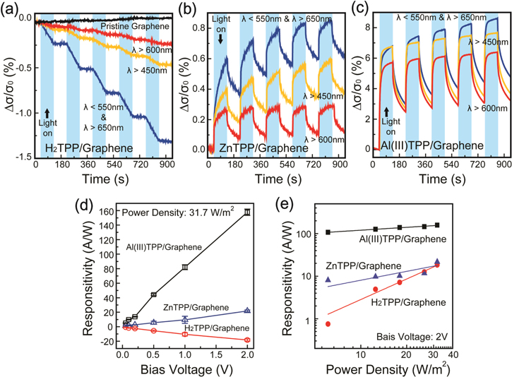
Figure 5. The real-time photocurrent obtained for the graphene-based photodetectors. (a) Time-dependent photocurrent of pristine graphene-based (black line) and H2TPP/graphene-based devices; band pass filters of λ > 450 nm (yellow line), λ > 600 nm (red line), λ < 550 nm and λ > 650 nm (blue line) were employed in the measurements. The photocurrent of (b) ZnTPP/graphene- and (c) Al(III)TPP/graphene-based photodetectors. (d) Photoresponsivity of H2TPP-, ZnTPP-, and Al(III)TPP-graphene-based devices as a function of the source-drain bias voltage during exposure to light with a power density of 31.7 W m−2. (e) Photoresponsivity as a function of the light power density; a bias voltage of 2 V was used for the measurements.
Download figure:
Standard image High-resolution image
In this work, a halogen lamp and band pass filters (BPFs: λ > 450 nm, λ > 600 nm, λ < 550 nm and λ > 650 nm) were used for the photoresponse measurements. The photoresponse of a pristine graphene-based device was also evaluated (see figure 5(a)), and no obvious current change was observed when compared to the graphene-organic devices. At a 50 mV bias voltage, the H2TPP-, ZnTPP-, and Al(III)TPP-graphene devices exhibited photoresponsivities of 0.22 A W−1, 0.54 A W−1, and 5.36 A W−1, respectively. Here, the photoresponsivity was calculated according to the expression R = (Photocurrent (A))/(Incident Optical Power (W)) = Iph/P0. The obtained photoresponse values are higher than those reported for other devices based on pure graphene monolayers [46–48]. Figure 5(d) shows typical photoresponsivity data for H2TPP-, ZnTPP-, and Al(III)TPP-graphene devices as a function of the source-drain bias voltage during exposure to light with a power density of 31.7 W m−2. As expected, the magnitude of the photoresponses increased as the optical power density increased. The photocurrent measured at a 2 V bias voltage was also plotted as a function of the incident optical power density; the results are displayed in figure 5(e). For these experiments, we used five graphene photodetectors for each case and repeated photodetecting experiments ten times demonstrating the repeatability of our results. It was found that the photocurrent behavior could be fitted by a simple power law expression [49–51], Iph ≈ APx, where Iph, A, and P are the photocurrent, proportionality constant, and optical power of the light source, respectively. The exponent x in the power law equation is affected by the density of trap states between the Fermi level and the conduction band of H2TPP, ZnTPP, or Al(III)TPP on the graphene surface [49]. Such non-unity exponential photocurrent behavior at different illumination powers could be ascribed to a complex process of electron (hole) generation, trapping, and recombination within the graphene and organic layers [52]. Upon fitting the results, x values of 0.69 and 0.22 were obtained for the ZnTPP- and Al(III)TPP-graphene-based devices, respectively. However, in the case of the metal-free H2TPP-graphene photodetector, data fitting yielded an x value of 1.6. Such findings imply that the simple metalation procedure developed in this work is an efficient strategy to fabricate different types of graphene photodetectors.
3. Conclusion
In summary, we successfully demonstrated a simple and easy controllable approach for the fabrication of photodetectors based on graphene-organic hybrid thin films. Here, metal-free H2TPP or metalloporphyrins (Al(III)TPP and ZnTPP) synthesized by a metalation process were utilized for tunable functionalization of the graphene-based devices. At a 50 mV bias voltage, H2TPP-, ZnTPP-, and Al(III)TPP-graphene photodetectors exhibited photoresponsivities of 0.22 A W−1, 0.54 A W−1, and 5.36 A W−1, respectively. The synthesis technique described in this report is a facile and efficient approach for fabricating graphene-organic hybrid thin films, which will be in demand for future transparent and flexible photodetector applications.
Acknowledgments
This research was supported by a grant (2011-0031636) from the Center for Advanced Soft Electronics under the Global Frontier Research Program of the Ministry of Science, ICT and Future Planning, Korea. We would like to acknowledge the financial support from the R&D Convergence Program of NST (National Research Council of Science & Technology) of Republic of Korea.