

Abstract
This work reports on the label-free electrical detection of DNA molecules for the first time, using silicon carbide (SiC) as a novel material for the realization of nanowire field effect transistors (NWFETs). SiC is a promising semiconductor for this application due to its specific characteristics such as chemical inertness and biocompatibility. Non-intentionally n-doped SiC NWs are first grown using a bottom-up vapor–liquid–solid (VLS) mechanism, leading to the NWs exhibiting needle-shaped morphology, with a length of approximately 2 μm and a diameter ranging from 25 to 60 nm. Then, the SiC NWFETs are fabricated and functionalized with DNA molecule probes via covalent coupling using an amino-terminated organosilane. The drain current versus drain voltage (Id–Vd) characteristics obtained after the DNA grafting and hybridization are reported from the comparative and simultaneous measurements carried out on the SiC NWFETs, used either as sensors or references. As a representative result, the current of the sensor is lowered by 22% after probe DNA grafting and by 7% after target DNA hybridization, while the current of the reference does not vary by more than ±0.6%. The current decrease confirms the field effect induced by the negative charges of the DNA molecules. Moreover, the selectivity, reproducibility, reversibility and stability of the studied devices are emphasized by de-hybridization, non-complementary hybridization and re-hybridization experiments. This first proof of concept opens the way for future developments using SiC-NW-based sensors.
Export citation and abstract BibTeX RIS
Introduction
In the field of point of care diagnostics (POC), the fast and direct detection of small quantities of biomolecules improves the early medical diagnosis of certain serious diseases such as cancer. It can also be used to detect the presence of pathogenic viruses or GMOs in the food industry, environmental protection and bio-defense in situ. In view of this, many research projects are conducted on portable nanoelectronic devices based on semiconducting nanowires (NW) [1]. Due to their high surface-to-volume ratio, which enhances sensitivity, these 1D nanostructures are ideal active elements for biosensor applications. In particular, nanowire-based field effect transistors (NWFETs) have been the subject of intense research during the past decade, because they can achieve the very sensitive, real-time, label-free electrical detection of several kinds of biochemical species such as DNA, proteins and ions [2–4]. Most of these NWFETs are Si-NW-based [4], mainly due to the compatibility of Si NW processing with the microelectronics industry. Despite the decisive advantages of these Si NWFETs for sensing applications, issues relating to the weak stability of Si in aqueous and saline media in the long term [5, 6] cause the drift of the signal and a low signal-over-noise ratio. Accordingly, industrial biomedical applications are strongly compromised. That is why alternative NW materials offering excellent electronic properties as well as inherent chemical robustness, non-toxicity and biocompatibility are under investigation. For instance, in view of DNA detection, some recent studies have focused on NWFET sensor devices based on GaN NWs [7], doped graphene [8, 9] or carbon nanotubes [10, 11]. In this context, silicon carbide (SiC) is a promising semiconductor for such nanodevices. Efficient SiC-based FETs have been reported due to SiC's wide band gap (2.36 eV for 3C-SiC) and relatively high electron mobility (900 cm2 V−1 s−1 for 3C-SiC) [12, 13]. Recently, our group has fabricated SiC NWFETs based on different variants of SiC nanostructures such as SiC NWs, SiC nanopillars (NPs) and Si-SiC core–shell NWs. The 3C-SiC NPFETs exhibited an experimental electron mobility value of 232 cm2 V−1 s−1, which is the highest value reported in the literature [14]. The main advantage of SiC over its non-Si-based counterparts is its ability to grow a stable thermal oxide (SiO2), which makes SiC directly compatible with the current usual Si technology. Moreover, mostly due to its chemical inertness, SiC is a highly stable and biocompatible material [15], currently used in the biomedical field as a coating for implants [16, 17] or as an electrode for the brain machine interface [18] where long-term use is needed. SiC NWs are envisaged to enhance cellular reproduction in tissue regeneration [19] and also to be used in nanoelectronics in harsh or biological environments [20–22]. SiC has been proven to be the most robust nanomaterial that the body does not recognize and reject as foreign (i.e., not organic) [23], and therefore opens the way to improve long term in vivo detection, applied to human health.
The present paper reports on SiC NWFETs fabrication to assess SiC NW sensing capacities for label-free electrical DNA detection. To the best of our knowledge, no device taking advantage of SiC NWs for the electrical detection of biomolecules, and particularly DNA molecules, has already been reported. In the literature, SiC exhibiting various morphologies has already been used for different kinds of detection. Planar SiC FETs have been used to achieve the electrical detection of gases [24–26]; SiC nanoparticles were used for in vivo pH measurements using fluorescence [27]; Yang et al used nanocrystalline 3C-SiC electrodes for electrochemical bio-sensing applications [28]; and Williams et al selectively functionalized SiC NWs for protein immobilization, but without reaching the step of the electrical detection of bioanalytes [29].
In this paper, the main steps of SiC NWFET sensor fabrication are described: the SiC NWs are grown by a bottom-up approach, the NWFETs are then elaborated, and localized functionalization is carried out. The early results are reported regarding the electrical detection of DNA grafting and hybridization using SiC NWFET devices as resistors. In NWFETs, the NW is used as the channel connector between the source and drain contacts. DNA is negatively charged due to non-protonated phosphate groups. When covalently grafted onto the surface of an n-type semiconductor NW, these negative charges can deplete the volume of the NW and reduce its conductance through the field effect mechanism. This effect is the basis of electrical DNA molecule detection. In this study, the as-grown SiC NWs are highly unintentionally n-doped, leading to a majority carrier concentration value of the order of 1019 cm−3. The doping level of the NWs influences the sensor response in both FET and resistor configurations. On the one hand, Zheng et al proved that when increasing the dopant concentration, the conductance of the device increases due to the decrease of the contact resistance which dominates NW conductivity [30]. On the other hand, Nair and Alam explain that the sensitivity of the sensor increases while the doping level decreases [31].
Methods
SiC nanowire growth
Semiconductor NWs are generally synthesized via a vapor–liquid–solid (VLS) process [32]. In this study, SiC NWs are grown by VLS on (100) oriented Si substrate in a home-made induction-heated vapor phase epitaxy (VPE) reactor at atmospheric pressure, using diluted (3%) propane and silane as precursors, purified Pd H2 as a carrier gas, and Ni as a catalyst [33]. The Si substrate is first etched with hydrofluoric acid to remove the native oxide and then coated with a 2 nm thick nickel layer by e-beam evaporation. A Ni-Si eutectic is formed at the melting point of 1100 °C for 2 min to achieve catalyst dewetting, leading to small liquid Ni-Si droplets on the substrate surface. Then, the precursors are introduced into the growth chamber for 5 min. The obtained SiC NWs are highly non-intentionally n-doped and appear to be well distributed on the substrate, exhibiting needle-shaped morphology with a length of approximately 2 μm and a diameter ranging from 25 to 60 nm (figure 1(a)). The structural properties of the NWs were analyzed by transmission electron microscopy (TEM), both in high angle annular dark field (HAADF) STEM mode (figure 1(a)) and in zero-loss filtered TEM mode (figure 1(b)). NW tapering, due to the shrinking of the NW section and the piling up of growing NW segments, as well as sidewalls with zigzag faceting [34] are observed. The crystalline structure belongs to SiC in its cubic 3C phase, with a 〈111〉 growth axis. The occurrence of planar defects due to stacking faults on the {111} planes, perpendicular or at an angle of about 20° to the NW axis, is observed—as is commonly found in 3C-SiC fibers [35].

Figure 1. (a) Top: scanning electron microscopy image of VLS-grown SiC NWs. Bottom: high angle annular dark field (HAADF) STEM image acquired near the tip of a single NW. Scale bar 100 nm. (b) Zero-loss filtered TEM image, taken along the 〈110〉 zone axis, showing stacking faults perpendicular and at 20° to the NW axis. The inset shows a detail of the 3C-SiC crystalline lattice (taken near the upper left-hand corner of the TEM image).
Download figure:
Standard image High-resolution imageSiC nanowire field effect transistor fabrication
In contrast with Si NWFETs, only a few papers have reported on SiC NWFET fabrication, and their experimental electrical performance is still low compared to their theoretical one [36]. The best values of effective mobility reported in the literature are 16 cm2 V−1 s−1 in the case of VLS-grown SiC NWs [37], and 232 cm2 V−1 s−1 in the case of SiC NPs [14]. This difference in mobility value is explained by the fact that the top-down approach used to etch NPs into a high-quality SiC epilayer leads to very low crystalline defect densities in the NPs [38] compared to NWs obtained by the bottom-up approach. Due to the many stacking faults, as shown in figure 1(b), VLS-grown SiC NWs exhibit a lower mobility value than the NPs. Nevertheless, the length of the NPs (around 500 nm) is long enough to integrate them into an FET, although it is too small to provide a sufficient functionalization surface in the case of a sensor. Therefore, in this study, the previously described VLS-grown SiC NWs have been chosen.
Our group developed an adapted technological process to integrate different variants of SiC NWs into back gate FETs [39]. The technological process involves the use of macro-contacts and micro-contacts to connect the NWs. Due to their short length, a window of macro-contacts is previously defined using optical lithography while the e-beam is only used to pattern the micro-contacts after NW deposition (figure 2). Before the micro-contact fabrication steps, the SiC NWs are cleaned in two HF 5% baths to remove the silicon dioxide layer formed by immersion in the gold etch solution used to eliminate the metal catalyst material remaining on the substrate after VLS growth. Immediately afterwards, the NWs are dispersed in an isopropanol solution by sonication of the substrate. A droplet of the NW solution is spread on a 200 nm thick SiO2 grown on Si substrates, previously prepared with macro-contacts and alignment markers (figure 2(a)). Thanks to the markers, the NWs are localized using scanning electron microscopy. A pattern is drawn and e-beam lithography is used to contact the NWs (figure 2(b)). First, a resist layer is spin-coated, exposed and developed. Then, two metal layers (Ni 5 nm, and Au 95 nm) are successively evaporated. Finally, a lift-off step is performed to remove the resist and to form the source and drain micro-contacts (figure 2(c)) [39]. With this design, it is possible to prepare up to 10 FETs on a single chip. As the electrical measurements are performed using a four-probe station in a dry state, an additional deposition step for insulating layers to protect the contacts is not necessary.

Figure 2. Fabrication steps for the micro-contacts of the NWFETs into a window of macro-contacts: (a) dispersion of the NWs, (b) design of the micro-contacts by e-beam lithography and then (c) the metallization of the micro-contacts by Ni-Au evaporation and lift-off to form the source (S) and drain (D) contacts.
Download figure:
Standard image High-resolution imageAfter fabrication, the NWFETs are electrically characterized at room temperature in ambient air using a semiconductor parameter analyzer (Keithley 4200). The probes of the analyzer are connected to the macro-contacts to bias the source and drain while the chuck is connected to the back gate. First, to check the stability, the drain current is monitored for 1 h without experiencing any significant drift. The obtained drain current versus drain voltage Id–Vd characteristic (figure 3(a)) is typical of NWFETs with non-annealed contacts, in which the transistors exhibit symmetric but non-ohmic behavior. No hysteresis is observed proving the low density of the mobile charges inside the SiC NWs. The drain current Id passing through the NWs for a drain voltage of 1 V is typically equal to 18 nA. Similar measurements are performed for different values of back gate voltage Vg (figure 3(b)). The back gate effect is low, but meaningful. Id varies from 3 to 7 nA for a Vg varying from −10 to 10 V (Vd fixed at 0.5 V).
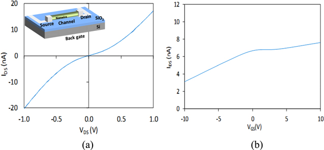
Figure 3. (a) Id–Vd characteristic of a SiC NWFET at Vg = 0 V. The insert is a schematic of the device; the SiC NW acts as a channel. (b) Id–Vg characteristic at Vd = 0.5 V.
Download figure:
Standard image High-resolution imageThe high carrier concentration explains the weak gating effect of the devices. Indeed, as the depletion region width is much smaller than the NW radius, the NW never becomes fully depleted in the off-state (also observed in [12]). Therefore, the change in the drain current is not monitored in the subthreshold regime [1], but in the linear regime. Moreover, due to the low effect of the back gate on the drain current, the gate electrode is not used to tune the sensor sensitivity, and then, Vg is grounded during the following experiments. As a consequence, the NWFETs are used in a resistor configuration, as in other similar studies [40].
SiC NWFET sensor fabrication
DNA sensors are affinity-based sensors. They rely on the high specificity and affinity between immobilized DNA probes (also called receptors) and complementary DNA targets to be detected, through specific hydrogen bonds. In view of this, DNA probes must be immobilized using an appropriate and localized functionalization process. This step is an essential part of the work since it strongly influences the sensor performance [41]. In a preliminary study, we developed a functionalization process on different SiC structures such as planar 6H-SiC surfaces, 4H-SiC etched nanopillars, core–shell Si/SiC nanopillars and single SiC nanowires [42]. The functionalization process is based on the grafting of an amino-organosilane on the SiC surface. The amino-organosilane is the aminopropyltriethoxysilane (APTES) deposited via chemical vapor deposition (CVD) in anhydrous conditions (under argon gas). On the one hand, vapor deposition is chosen because it creates more reactive self-assembled monolayers than liquid deposition [43]. On the other hand, anhydrous conditions enable APTES deposition to be controlled, consuming the water molecules naturally present on the SiC surfaces and the hydroxyl sites (Si-OH) also on the SiC surface. It is to be noted that un-passivated and OH- dangling bonds on the SiC surface can act as surface trap states, the effects of which are detrimental for electrical characteristic measurements, as demonstrated in Si NWFETs [44]. The APTES film presence on the SiC surface was checked by XPS analysis [45]. Elsewhere, films made of other kinds of silane deposited on 6H-SiC planar surfaces have been thoroughly characterized by Schoell et al [48]. In our study, APTES deposition is followed by the grafting of glutaraldehyde as a cross-linker between the amine terminations of both the APTES and the DNA probes thanks to its double aldehyde termination. Then, covalent DNA probe grafting on the glutaraldehyde is performed via a reduction step modifying the imine bonding into an amine one. The DNA probe is a 20-base pre-synthetized oligonucleotide sequence 5' NH2-C6-TTTTTGATAAACCCACTCTA 3'. Finally, the DNA target molecules are complementary single-strand DNA that fully hybridize with the DNA probes to create double-stranded DNA. The complementary target strand sequence is 5'-CATAGAGTGGGTTTATCCA-3'. We have previously studied and validated DNA grafting and complementary hybridization on various SiC nanostructures using different characterization techniques such as XPS, fluorescence microscopy and AFM [42, 45]. Furthermore, to test the selectivity of the sensors, hybridization with non-complementary DNA targets is performed. The non-complementary strand sequence is 5' CATCTCACTAACGCGGTCA 3'.
In the present study, in view of confining the probes and target molecules on the SiC NW sensitive area, the functionalization process described above is locally performed on the chip by combining e-beam lithography and the chemical modification of the SiC NW surface (figure 4). This original process enables two SiC NW sensing devices to be built simultaneously on the same chip: a functionalized one, which is the DNA sensor (DEV1), with another one, which is not functionalized, acting as a reference device (DEV2). Both devices are close to each other (d < 10 μm). Accordingly they undergo the biochemical treatment (DNA grafting, hybridization and de-hybridization) in the same conditions.

Figure 4. A flow-chart of the localized functionalization process used for DNA grafting and hybridization on the SiC NW nanosensor (DEV1: functionalized device), while the other one (DEV2: reference) is kept un-functionalized. After photoresist deposition and e-beam lithography (1), the localized functionalization process is performed on DEV1. This involves a silanization (APTES) step (2) followed by crosslinker grafting with glutaraldehyde (3). After lift-off (4), covalent DNA probe grafting (5) followed by DNA hybridization (6) on the SiC NW are carried out.
Download figure:
Standard image High-resolution imageFirst, polymethylmetacrylate (PMMA) resist is spin-coated onto the chip. Then, a 10 × 10 μm2 cavity is opened around DEV1 thanks to e-beam lithography. The precision of this technique allows DEV1 to be functionalized while DEV2 is kept protected under the resist and is thus unmodified (step 1 in figure 4). After the opening step, soft O2/air plasma exposure enhances DEV1's surface reactivity without removing the resist. In view of silanization (step 2, figure 4), the chip is placed in a chamber containing 150 μl of APTES (Sigma-Aldrich) sealed under a low humidity atmosphere (1% relative humidity). The chamber is placed in a furnace at 80 °C for 1 h. Then, the chip is rinsed with dry ethanol and annealed at 110 °C for 1 h. The chip is immersed in a 25% glutaraldehyde (Sigma-Aldrich) water solution for 1.5 h (step 3, figure 4). After glutaraldehyde rinsing, the functionalization process of DEV1 is achieved, making it ready for DNA grafting contrarily to DEV2. A lift-off step performed in an acetone bath for 45 min removes the resist from the chip surface, releasing DEV2 (step 4, figure 4). A drop of solution containing the 20-base DNA probe molecules (purchased from Biomers, Germany) diluted in a grafting solution to a concentration of 10 μmol l−1 is deposited on both devices. The N=C bonds are stabilized through a reduction step in a NaBH4 solution (0.1 mol l−1) for two hours (step 5, figure 4). Even if the probe drop is deposited on both devices, DNA probe grafting is only effective on DEV1. Complementary or non-complementary hybridization is performed on both transistors with a 2 μmol l−1 DNA target solution for 45 min at 42 °C under a wet atmosphere (step 6, figure 4). Rinsing steps with sodium citrate salt solution (SSC) 2X and 0.2X are carried out on the SiC NWFET sensor to remove unbound DNA targets from the surface. Finally, the devices are dried with nitrogen gas and are ready for the electrical characterizations, which are performed at room temperature and at an ambient humidity level (60%–70% relative humidity). The experience of DNA de-hybridization is performed thanks to the DNA denaturation process, immersing the chip in a NaOH (C = 0.1 μM) solution for 45 min; afterwards the hybridization step can be reiterated. The whole process is performed on all the devices fabricated on a single chip.
Results and discussion
Similar to some studies [10, 11], and as mentioned above, the detection measurements are performed in a dry state, after rinsing with diluted solutions leading to a reduced DNA counter ion concentration. As a result, the anionic charges of the DNA are essentially balanced by the depletion layer in the NW subsurface. This is supported by the simulation study of Nair and Alam, showing that dry state measurements lead to enhanced sensitivity in the case of the detection of negatively charged molecules with n-doped NWs [31]. This also avoids the uncontrolled effects of both micro-fluidics and ionic liquid, such as the liquid flow and Debye length, respectively.
First, the drain current versus drain voltage (Id–Vd) characteristic of DEV1 is measured between −1 and 1 V before (initial state) and after DNA probe grafting (step A), and then after complementary DNA hybridization (step B) (figure 5). Compared to the initial state, the current is systematically lowered upon DNA grafting and hybridization, while the shape of the characteristic does not change. Upon grafting, the current decreases from 14.72 nA to 12.01 nA, while upon hybridization, the current decreases until 11.25 nA. This trend confirms that the sensor current is affected by the field effect caused by the DNA molecules. In agreement with an n-type-doped SiC NW, the channel is depleted and the current decreases after each step.
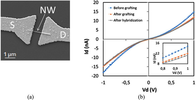
Figure 5. (a) A SEM view of the SiC NW (diameter 50 ± 5 nm, length 2 μm) between the source and drain contacts. (b) Id–Vd characteristic of a SiC NWFET (DEV1) at Vg = 0 V at three different steps: before DNA probe grafting (initial state), after DNA probe grafting (step A) and after hybridization with the DNA targets (step B). The insert shows a zoom of Id–Vd.
Download figure:
Standard image High-resolution imageSecond, for a more complete sensor operation test, the Id–Vd characteristic of two typical devices DEV1 (sensor) and DEV2 (reference) are measured simultaneously between −1 and 1 V after successive and important steps which are labelled from A to E: after silane and glutaraldehyde covalent bonding (initial state), after probe DNA grafting (step A), after DNA hybridization with the complementary DNA target (step B), after de-hybridization (step C), after hybridization with non-complementary DNA targets (step D), and after re-hybridization with complementary targets (step E). These modification steps are reported horizontally in figure 6.

Figure 6. Plot of the drain current evolution (Vd = 1 V, Vg = 0 V (resistor configuration)) of both the functionalized SiC device (DEV1 as the sensor, cross symbol) and the un-functionalized one (DEV2, as the reference, square symbol) after different modification steps: (initial step) after silane and glutaraldehyde covalent bonding, (A) after DNA probe grafting, (B) after complementary hybridization, (C) after de-hybridization, (D) after non-complementary hybridization and (E) after complementary re-hybridization. The percentages represent the variation of the mean current between two successive steps.
Download figure:
Standard image High-resolution imageTwo other SiC NWFETs, named DEV1' and DEV2', from the same chip are also investigated. Similar to DEV1 and DEV2, the characteristics of both DEV1' and DEV2' are simultaneously measured after successive and important steps. However, in contrast with DEV1 and DEV2, the cycling modification steps are done in order to focus on the re-usability and robustness of SiC NWs, notably after several DNA de-hybridization treatments using NaOH. Accordingly, electrical measurements are made after silane and glutaraldehyde functionalization (initial state), after probe DNA grafting (step A'), after DNA hybridization with complementary DNA target (step B'), after de-hybridization (step C'), after hybridization with complementary DNA targets (step D'), and after de-hybridization (step E'). These modification steps are reported horizontally in figure 7. For all devices, to ensure measurement reliability, the characteristic is repeated seven times (in the case of DEV1 and DEV2) or ten times (in the case of DEV1' and DEV2') at each step. Then, the Id current value for a source-drain bias of 1 V is recorded and its mean value is calculated based on the seven or ten measurements. The evolution of drain current after the different modification steps (from step A to step E) is reported for both DEV1 and DEV2 in figure 6, while the one of both DEV1' and DEV2' is reported in figure 7 (from step A' to step E'). Prior to studying the effects of DNA grafting and hybridization on the current, two preliminary results are reported regarding the effects of both APTES and glutaraldehyde functional layers and salts for both devices.

Figure 7. Plot of the drain current evolution (Vd = 1 V, Vg = 0 V (resistor configuration)) of both the functionalized SiC devices (DEV1' as the sensor, cross symbol) and the un-functionalized one (DEV2', as the reference, square symbol) after different modification steps: (initial step) after silane and glutaraldehyde covalent bounding, (A') after DNA probe grafting, (B') after complementary hybridization, (C') after de-hybridization, (D') after complementary hybridization and (E') after de-hybridization. The percentages represent the variation of the mean current between two successive steps.
Download figure:
Standard image High-resolution image
First, compared to the initial SiC NWFETs, a weak and meaningless effect of the APTES and glutaraldehyde layers on the electrical characteristics is reported. These layers do not involve charged species. Particularly regarding APTES, we previously showed using XPS analysis that the fraction of protonated amine was negligible [45]. So, as expected, these layers do not contribute to the provision of a significant field effect.
Second, any contribution made by the charged salts contained in the electrolyte solutions (used to graft or hybridize DNA) on measured currents has been assessed. Indeed, in spite of the rinsing steps before drying (see experimental parts), it cannot be excluded that some residual salts may still be adsorbed on the SiC NW surface. So, these charged species may have an influence on the field effect. In view of this, grafting experiments are performed using the common grafting solution but without the DNA molecules. After rinsing and drying, no significant current variation in electrical characteristics is reported. Therefore, the influence of residual salts contained in electrolyte solutions and buffers does not contribute significantly to the signal.
In the case of DEV1 and DEV2 (figure 6), the mean drain current value of the sensor (DEV1) decreases by 21.9% after DNA probe grafting (step A), while it decreases by 7.1% after hybridization (step B). Upon these first two steps, the current of the reference device (DEV2) does not change by more than ±0.6%. This means that the sensor response of 7.1% obtained after hybridization is significant enough to conclude that the detection of DNA targets is effective. It also confirms the absence of DNA molecules attached or adsorbed to DEV2. Similar trends and current variations (in %) upon DNA grafting and hybridization are obtained for DEV1' and DEV2', as can be observed in figure 7 (step A' and step B'). A mean current value decrease of 21.2% is obtained upon grafting while a decrease of 8.1% is obtained upon hybridization. The difference between the devices comes from absolute values of current, which are higher for DEV1' and DEV2'. This difference mainly comes from the geometry of the SiC NWs (diameter and length). In addition, depending on the way they are contacted, some differences in contact resistance may leverage the electrical properties. In spite of these differences, comparing the behavior of DEV1 and DEV1', the signal related to DNA hybridization (drain current decrease) is systematically lower than the signal related to DNA grafting. Such a trend is in agreement with the one obtained elsewhere by several authors. S Ingebrandt et al obtained a lower decrease in drain current upon DNA hybridization compared to the one measured after DNA grafting [46] on Si NWs. A similar observation is reported with the DNA immobilized on field effect sensors modified with a charged weak polyelectrolyte layer [47].
Here, the ratio between the current decrease obtained upon DNA probe grafting (21.9%) and hybridization (7.1%) in DEV1 is approximately 3. Similar results are obtained for DEV1'. Accordingly, knowing that the electric charges of both DNA targets and DNA probes are equivalent, it can be assumed that only one third (33%) of the DNA probe molecules attached to the SiC NW hybridize with the DNA targets. This estimated hybridization rate is in agreement with other published values obtained by various detection methods such as fluorescence measurements on DNA modified latex microparticles [49], electrochemical analysis on DNA modified gold electrodes [50], or by surface plasmon resonance on DNA modified gold substrates [51]. To explain this estimated hybridization rate, different factors can be involved. Morphological factors may influence and limit the hybridization rate such as an important DNA probe surface density on the sensitive NW surface, a steric hindrance limiting the DNA target accessibility to immobilized probes, and the DNA probe orientation and conformation [50, 51]. Other factors involve the depletion region and its restrictive expansion within the finite SiC NW diameter. Accordingly, the observed current value corresponding to DNA hybridization (figure 6, step B) would correspond to a bottom threshold value, even though the effective DNA hybridization rate is superior to 33%. In this case, the calculated hybridization value of 33% would be underestimated. Obviously, further investigation is necessary to determine which one of the suggested factors limits the estimated hybridization rate and thereby the sensor sensitivity. On the one hand, varying the DNA probe surface density and thereby its solution concentration would emphasize its influence on the hybridization rate. On the other hand, experiments which consist of varying the SiC NW diameter would enable us to know its influence on the hybridization rate. Some studies on the NW diameter dependence of sensitivity to the surface charges have been performed on Si NWs [52–54]. According to them, it seems that using diameters as thin as 20 nm improves the detection limit [52], although this result is controversial according to other groups' studies [53, 54].
To further investigate both the reversibility and selectivity of DNA hybridization on the SiC NWs, successive and step-by-step experiments are carried out on DEV1 and DEV2 (steps C to E in figure 6). First, following the previously described hybridization step (step B), a de-hybridization step is carried out (step C). While no significant current variation is observed for DEV2, a 2.5% increase of the mean current is obtained for DEV1. This is in agreement with the removal of DNA targets. However, it seems that only a fraction of the targets is removed. Indeed, theoretically, the current increase should be equal in absolute value to the decrease recorded after the previous hybridization step (step B), which is about 7%. The observed discrepancy might be due to the relative efficiency of the used denaturation process, leaving some double-stranded DNA still present among the single strands on the SiC NW surface. Second, to check the selectivity of the sensor, the next hybridization experiment is performed using non-complementary DNA targets (step D). The resulting change in the mean current is only +0.5% in DEV1, which is not significant compared to the +1.2% obtained for the reference (DEV2). This negligible change in current demonstrates the selectivity of the sensor. Third, a further hybridization is performed with complementary DNA targets (step E). As can be observed, the current decreases in the opposite direction than for the previous de-hybridization (step C) with a close absolute value of 2.3%. This is in agreement with the hybridization process involving a fraction of free DNA single strands.
To summarize, the entire current evolution along the successive steps (hybridization/de-hybridization/non-complementary hybridization/hybridization) is in accordance with the expected effects of each step on DEV1. The current evolution shows both the selectivity and reversibility of DEV1 in the SiC NWFET sensor. The reversibility of the process is further confirmed when carrying out successive hybridization/de-hybridization cycles on DEV1' (steps C' to E' in figure 7). Following the hybridization step on DEV1' (step B') already described, the de-hybridization step is accompanied by a current increase of 7.4% (step C'), which is equivalent to the current decrease of 8.1% obtained after hybridization (step B'). These current variations being similar in absolute values, the de-hybridization process seems to be more efficient than for DEV1 (step C in figure 6). Then, the following re-hybridization and de-hybridization steps are accompanied by a current decrease of 14.6% and an increase of 9.1%, respectively. As in the case of DEV1, the current variations observed for DEV1' are significant compared to the weak current variations obtained for DEV2'. Moreover, they are in agreement with the expected effects of each step on DEV1'.
Elsewhere, for all devices, all these steps are done over two or three days, depending on the device, and no significant drift of current is observed over such a period (figures 6 and 7). Therefore, the stability of SiC NWFET sensors during this period is demonstrated. These experiments show the re-usability and robustness of SiC NWs, notably after several courses of DNA de-hybridization treatment using NaOH. The high stability of SiC in a saline solution is therefore also demonstrated. Further experiments will have to extend this period over more time (weeks and months). Finally, we have shown a proof of the concept using SiC NWFETs for the electrical detection of DNA hybridization. These preliminary results also show the selectivity, reversibility, re-usability, and high stability—both in time and in saline solution—of these advanced devices.
Further challenging experiments will have to go deeper into the role of some of the important characteristics of SiC NW sensors on the final device's electrical sensing performance. These concern (i) the electrical properties of SiC NWs, (ii) the functional layer and (iii) measurement conditions. First, optimizing the VLS growth conditions of SiC NWs will enable their electrical characteristics and conductivity to be improved by eliminating stacking faults (figure 1(b)) and reducing the unintentional doping level. Second, the organic functional layer characteristics (e.g. chemical structure, chain length) strongly influence the sensing performance, as has been shown in molecularly modified Si NWFETs for gas sensors [55, 56]. In our study, the functional layer involves APTES and glutaraldehyde layers as well as DNA probes. We plan the replacement of APTES and glutaraldehyde layers with a unique molecule such as glycidyloxypropyl-trimethoxysilane (GOPS), which will present several advantages. On the one hand, the functionalization process will be less time consuming than at present and will enable the use of toxic glutaraldehyde to be avoided. On the other hand, it will allow us to shorten the number of C length chains of the functional layer (from 9 to 6). As a consequence, by reducing the distance between the DNA and the SiC NW surface, a better field effect is expected, providing more sensitive devices. Furthermore, the functionalization process leading to GOPS deposition will have to be carefully controlled in order to avoid the presence of unpassivated surface hydroxyl (Si-OH and OH-) ions at the SiC surface, as they act as surface trap states which are strongly detrimental to electrical analysis [44, 56]. Third, the DNA conformation and structure are strongly dependent on the surrounding humidity level [57, 58]. Humidity-induced DNA conformation changes on the SiC surface will leverage the field effect. So, the study of humidity level variation on the device's electrical characteristics will enable us to investigate the influence of DNA conformation change on these characteristics. Finally, besides the sensitivity and limit of detection studies, a more real approach to the selectivity and discrimination capacity of our devices will be performed. More accurately, the effect of base-mismatched DNA targets [59, 60], as well as the confounding mixture with complementary and non-complementary DNA targets on current variations will be investigated.
Conclusion
This study presents the fabrication of SiC NWFETs from VLS-grown SiC NWs. This is followed by the original localized functionalization process of the SiC NWFETs, enabling electrical label-free DNA detection using a resistor configuration. The initial SiC NWFETs exhibit symmetric, non-ohmic Id–Vd characteristics. For the first time, electrical measurements performed after both DNA probe grafting and hybridization on SiC NWFETs show successive decreases in the mean drain current values. The selectivity, reversibility and the stability of the nanosensor are emphasized thanks to non-complementary DNA target hybridization experiments, and de-hybridization/re-hybridization cycling experiments. Once the properties of the SiC NWs are optimized, further investigation will include the sensitivity and limit of detection studies. In addition, a more real approach to selectivity and the discrimination capacity of our devices will be performed. These early results obtained for SiC NWFETs provide the basis for promising devices that will fully exploit the excellent properties of SiC, such as chemical inertness and biocompatibility.
Acknowledgments
The authors thank the members of the technical staff of the PTA facilities in Grenoble (France) for their technical support, and Gérard Ghibaudo (IMEP-LAHC) and Mireille Mouis for their attentive help. This work was supported by the European Network for Excellence NANOFUNCTION and by the French RENATECH network.