
Abstract
We present a method to characterize sub-10 nm capacitors and tunnel junctions by interferometric scanning microwave microscopy (iSMM) at 7.8 GHz. At such device scaling, the small water meniscus surrounding the iSMM tip should be reduced by proper tip tuning. Quantitative impedance characterization of attofarad range capacitors is achieved using an 'on-chip' calibration kit facing thousands of nanodevices. Nanoscale capacitors and tunnel barriers were detected through variations in the amplitude and phase of the reflected microwave signal, respectively. This study promises quantitative impedance characterization of a wide range of emerging functional nanoscale devices.
Export citation and abstract BibTeX RIS
1. Introduction
As device scaling continues below 20 nm [1, 2] and novel classes of nanodevices appear on the horizon [3–9], the accurate characterization and a detailed understanding of the electronic and capacitive properties of these devices are essential, yet challenging [10]. Nanocapacitors and tunnel barriers, which are building blocks in most memories [11–14], are becoming extremely difficult to characterize due to their sub-femtofarad capacitances. Macroscopic capacitances are typically measured in a bridge circuit configuration, wherein the signals across the device and the reference impedance are balanced in a feedback loop [15–19]. Such measurement setups inevitably include some cables that have a finite parasitic capacitance on the order of hundreds of picofarads and produce enormous attenuation of the test signal. Consequently, new techniques have emerged for attofarad measurement [20–25], including interferometric techniques with input signal in the GHz frequency to increase the measured admittance of tiny capacitors [26–28]. These techniques were combined with scanning microwave microscopy (SMM) [29–33], called here interferometric scanning microwave microscopy (iSMM [34]) to obtain attofarad resolution with the lateral resolution of atomic force microscopy (AFM) in the frequency range of 2–20 GHz.
Previous studies using ac-biased scanning probes [35–38] (e.g., tunneling microscope) have either shown 10 nm lateral resolution or performed quantitative studies on micrometer or sub-micrometer devices in the sub-femtofarad range. To date, no report has indicated the ability of such microscopes to perform quantitative studies of sub-10 nm diameter nanodevices. Here, we show that sub-10 nm diameter capacitors can be measured by a technique combining an 'on chip' calibration kit and a refined iSMM tip. This technique allows statistical studies of thousands of devices within a single acquisition—an important consideration—given the dispersion that is usually observed in the fabrication of nanoscale components. We also discuss the quantitative interpretation of the results for tunnel capacitors.
2. Samples and experiments
Among the various techniques used for sub-10 nm nanoelectrode fabrication [39–44], we selected a combination of advanced e-beam lithography and self-organization [44]. The nanocapacitors measured in this work were based on nanoscale gold electrodes (top diameter range of 5–100 nm), with an ohmic contact to a highly doped silicon substrate (figure 1(a)) [44, 45]. These gold electrodes, showing single crystal Au nanodot after thermal annealing, have a structure very close to that of ideal cuboctahedron or truncated octahedron nanoparticles [46]. After gold evaporation [44], silicon atoms, coexisting with gold, move to the surface during thermal annealing and form a SiO2 cap on top of the nanoelectrodes. During this process, the different Au dot dimensions produce different SiO2 thickness measured experimentally (see supporting information S1) and considered in finite element modeling (FEM). The advantage of this annealing process is that SiO2 covers only gold nanoelectrodes on silicon but not gold electrodes on thermal SiO2 used for the calibration kit. Typical SiO2 thickness over nanoelectrodes is however too thick (>5 nm) to generate and study tunnel effect. As a consequence, on a second type of samples, we have removed the SiO2 covering dots by dipping the sample into HF (5%) and formed a new insulating layer of Al2O3 by atomic layer deposition (with thickness of 0.5 nm and 5 nm). These samples are used to study the effect of tunnel current on impedance images. However the 'on-chip' calibration kit cannot be used in this case because it is recovered with Al2O3. The iSMM tip is operated as a top Pt electrode. Figure 1(b) shows a scanning transmission electron microscopy (STEM) image of a 5 nm diameter facetted nanocrystal that was used as the bottom electrode.
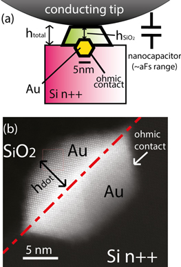
Figure 1. (a) Schematic cross-sectional view of the nanocapacitor under study and its equivalent circuit diagram. (b) STEM image of the bottom facetted gold electrode at atomic-scale resolution [44].
Download figure:
Standard image High-resolution imageThe iSMM was operated under typical ambient conditions. A relative humidity 45% ± 5% is controlled in the iSMM room. We prepared three different tips to evaluate a possible influence of the water meniscus [47–50] between the tip and surface that has been widely studied with scanning capacitance microscopy [47, 48]. Figure 2(a) shows a scanning electron microscopy (SEM) image of a commercial Pt probe (Rocky Mountain Nanotechnology© [51]). A convolution effect was clearly observed on the impedance image when this tip was used at 7.8 GHz with 100 nm diameter dots (figure 2(b)). The smallest dots (5 nm) were not observed (figure 2(c)). Coating the tip with a hydrophobic self-assembled monolayer of octanethiols (figure 2(d)) drastically reduced the convolution effects on impedance images at 7.8 GHz for 100 nm dots (figure 2(e)), although the 5 nm dots were still not observable (figure 2(f)). These results indicate that parasitic capacitances arising from the water meniscus have to be accounted for in the quantitative evaluation of nanoscale capacitors. In a third experiment, we reduced the initial tip dimensions by focus ion beam (FIB) structuration to obtain an ultrasharp Pt tip (figure 2(g); also see SI for methods). For large dots (figure 2(h)), convolution effects on the impedance image at 7.8 GHz were furthermore reduced. The point is that 5 nm dots could be distinguished (figure 2(i)). Therefore, tip refining is a relevant solution for impedance imaging of sub-10 nm diameter capacitors. The tips radii evaluations are given in supporting information (S2).

Figure 2. SEM images of three tips used in the experiments: (a) a commercial Pt tip (Rocky Mountain Nanotechnology© [51]), (d) a standard tip coated with a hydrophobic self-assembled monolayer (C8H17-SH), and (g) an ultrasharp tip refined by FIB. (b), (e), (h) |Smeas| amplitude images at 7.8 GHz for an 100 nm nanodot using these three tips acquired separately. (c), (f), (i) A digital zoom to highlight the 5 nm dot resolution in three cases. We did not zoom for the smallest dots when scanning because we need images with the calibration kit to deduce their capacitance values.
Download figure:
Standard image High-resolution imageNext, we integrated a calibration kit and the nanocapacitors on the same chip (figure 3(a)). The calibration kit comprised metallic electrodes on 120 nm thick thermal SiO2 (areas of 0.25 and 1 μm2). Their capacitances values were estimated by FEM as 121 and 369 aF, respectively. Figure 3(b) shows the iSMM image of the transmission coefficient amplitude |Smeas| in unit of dB in false color values at 7.8 GHz for the whole structure, obtained by using the standard SMM tip. Due to the extremely small dimension of our capacitors, iSMM images have 2048 × 2048 pixels. At typical scan rate of 0.08 line s−1, it takes about 7 h to get one image. As a consequence a small drift is observed. Thanks to calibration capacitors located all along the nanodots array, we compensated the drift effect coming from the scan duration by using the nearest calibration capacitors to determine the nanodots capacitances. With this approach, we expect to take into account the drift effect better than using only an initial calibration [52]. From scale rule, the |Smeas| values for the calibration kit were in the same range as the nanodots. As a first-order approximation (both our calibration kit and nanodots capacitances are in the sub-fF range), we determined a simple relationship between the capacitance and the Smeas parameters (see S3 for a detailed derivation):


Figure 3. (a) Schematic cross-sectional view of the experimental setup composed of the nanocapacitors under study, calibrated capacitors, and iSMM. (b) iSMM |Smeas| image at 7.8 GHz, including the nanocapacitors and calibrated capacitors. (c) Capacitance values estimated from equation (1) with calibration capacitances and simulated capacitances as a function of nanodot dimensions for standard tip. Inset is a cross-section view of electrical field lines and isopotentials simulated by FEM (COMSOL©) with Rm = 65 nm. (d) Experimental capacitance value corrected from the water meniscus contribution (solid circles) plotted for the different dot diameters. Capacitor values for the three tips obtained by FEM (Rm = 0 nm) plotted for comparison (solid squares). Inset image shows the limit of resolution of our system.
Download figure:
Standard image High-resolution imageThe calibration factor α obtained with equation (1) for the two calibrated capacitors was α ≈ 6 × 10⁻¹⁴ F. In linear scale, Δ|Smeas| corresponded to the variation of |Smeas|.
Surprisingly, although the variation of the capacitance between the nanodot tip and the substrate (ΔCiSMM) was small (see S4 for histogram), the extracted nanocapacitor values CiSMM were up to two orders of magnitude larger than those expected from theoretical estimations (figure 3(c)). Such a mismatch is likely related to parasitic capacitances that could arise from the tip cone/substrate capacitance or the water meniscus discussed previously. The first contribution has been calculated by FEM (see SI S9). Its effect is rather large (fF range) but it concerns both calibration capacitors and nanocapacitors, except a topography cross-talk of ∼ −0.08 aF nm−1 that well be further discussed below. At the opposite, the water meniscus affects only the nanocapacitors and not the calibration capacitors. The consideration of the presence of a water meniscus by FEM gives reasonable quantitative agreement with experimental results (figure 3(c)). We tried to inject nitrogen in the closed box of the iSMM, however images became unstable and little influence was observed. As reported in the literature, it is extremely difficult to remove the three first monolayers of water on silica surface [48, 50, 53], even using a hydrophobic self-assembled monolayer [54]. In the next section, we removed its contribution to extract the intrinsic capacitance values. The meniscus radius Rm was extracted from FEM (see S5) based on the measured capacitance between the tip and the substrate. We estimated Rm ∼ 65, 52, and 35 nm for normal, hydrophobic, and ultrasharp tips, respectively. It is in agreement with [47] where the estimated meniscus radii are 60–100 nm considering standard tips radii between 100 nm and 300 nm. As in [47], a simple straight line connecting the tip to the surface is used as meniscus edge (figure S6(a), (c)). The shape of the meniscus edge should not significantly affect the capacitance due to its high dielectric constant of water. However since we are not in a planar surface configuration (we study nanodots in our case), we derived a new simple analytic formula based on superposition theorem to extract a corrected value of the intrinsic nanodot capacitance in next section.
3. Results and discussions
We determined the intrinsic capacitances of the nanocapacitors (see S5 for detailed derivation) by supposing that Rm remained unchanged when the tip was on top of the nanodot:
where CiSMM is the measured capacitance of the nanocapacitor; Ctotal water is the estimated capacitance of the water meniscus between the nanodot and the Si substrate; and η (∼1.62) is the ratio of the total nanodot height to the SiO2 thickness on the nanodot  . For the smallest electrodes, the total height htotal is nearly 8 nm, and
  is ∼4 nm (figure 1(a)). Ccorrected is the capacitance corrected from the contribution of the water meniscus. εwater = 80 and
  = 3.9 are the dielectric relative permittivity values of water and SiO2, respectively.
Using this equation, we determined the calibrated capacitances in the range of few aF for the three different tips shown in figure 3(d) (solid circles), where the error bars were obtained from the full width at half maximum of the nanocapacitor capacitance histograms. The theoretical estimation of the capacitance for three tips (solid squares) were also calculated by FEM (with Rm = 0 nm; see S5). The small decrease of capacitance with increased nanodot diameter can be explained by (i) the constant contact area for dots >20 nm (below this nanocapacitor dimension, the iSMM tip are in contact with the whole dot area), and (ii) the increased SiO2 thickness with dot dimension, due to size-dependent SiO2 growth during the annealing process. Although most parasitic capacitance contributions should be canceled out by the aforementioned iSMM calibration, a small shift between experimental and FEM results in average 2.4 aF remains. Among the possible uncertainties, we have stray capacitance, the error in the determination of the tip radius, nanodot size, oxide thickness, and force applied by the tip. Here we focus on the topography cross-talk and setup resolution. Indeed there is a difference in height (120 nm) between calibrated capacitors and the substrate plane of nanodots. This suggests the evolution of the Cstray of ∼0.02 aF for 1 nm decrease in probe height. Accordingly, if the height is increased by one nanometer, the stray capacitance would be reduced by 0.02 aF. Based on ∼29.6 nm height difference between 100 nm dots and 10 nm dots, Cstray contribution for 100 nm dots (of height 37.5 nm) are ∼0.6 aF less than that for 10 nm dots (of height 7.9 nm), in agreement with results obtained with the standard tip (figure 3(d)). This estimated topography cross-talk (−0.02 aF nm−1) is in the order of magnitude, although lower, of the values we estimated by FEM (∼−0.08 aF nm−1) (see SI9) and reported in [52] (0.03–0.06 aF). Concerning the measurement accuracy (including the noise level) of the system, we did a similar measurement as in [31]. We obtained a 'white noise' contribution corresponding to a capacitance fluctuation of ∼1 aF and another fluctuation of ∼0.5 aF (upper right in figure S7(b)). The 'white noise' contribution can be drastically reduced using an averaging filter (typically used with the 'histogram' approach). Typically we plotted histograms with ∼500 samples (thanks to the 2048 × 2048 pixels images), which almost suppress this noise contribution. The other, unknown contribution cannot be removed. It sets the limit of resolution (∼0.5 aF) of our experimental setup.
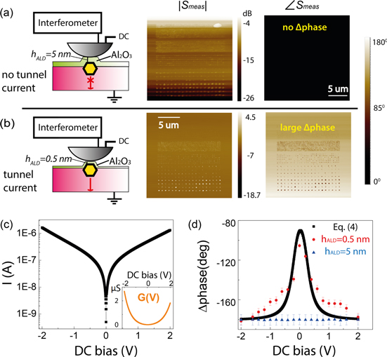
Tunnel barriers are another key element in memories. In advanced memory architectures such as for OxRAMs [14], resistive and capacitive effects are not static and a clear bias and real-time dependent impedance picture, at nanoscale, is of prime importance. To evaluate the impact of tunneling current on |Smeas| amplitude and phase, we used a second type of samples with 5 Å and 5 nm atomic layer deposition of Al2O3. As mentioned above, these samples are not compatible with the 'on-chip' calibration kit because of the loss of electrical contact on calibration capacitors covered with Al2O3. For 5 nm thick layer, a clear signal was only observed on |Smeas| (figure 4(a)) as for previous samples. For 5 Å thick layer, a clear signal contrast (up to 90°) appeared on the phase (figure 4(b)). To explain this observation we used a simple interferometer model (see S8) with a test device composed of a resistance in parallel with a capacitor:


where G0 = 0.25 μS and C0 = 306 aF are the reference conductance and capacitance, respectively, when Smeas = 0 (considering the water meniscus); Zc
= 50 Ω is the characteristic impedance; the constant e1 accounts for the loss in cables;  ; and cste = −270° is a constant phase related to the phase shift in cables. From equation (4),
  is expected to vary significantly with dc Bias V (from parameter G). Considering a model for the dc tunnel current I according to Simmons' model [55] (figure 4(c) is the I–V curve and inset is the G–V curve), reasonable agreement with experimental results on phase variation was obtained (figure 4(d)) by using equation (4). Typical parameters (relative electron mass Mr
= 0.16 and height of rectangular barrier φ = 3.1 eV) were considered for the I–V curve. For comparison, blue marks in figure 4(d) indicate that there is no bias dependence on the phase when the Al2O3 thickness is 5 nm (no tunnel current).
is expected to vary significantly with dc Bias V (from parameter G). Considering a model for the dc tunnel current I according to Simmons' model [55] (figure 4(c) is the I–V curve and inset is the G–V curve), reasonable agreement with experimental results on phase variation was obtained (figure 4(d)) by using equation (4). Typical parameters (relative electron mass Mr
= 0.16 and height of rectangular barrier φ = 3.1 eV) were considered for the I–V curve. For comparison, blue marks in figure 4(d) indicate that there is no bias dependence on the phase when the Al2O3 thickness is 5 nm (no tunnel current).
Figure 4. (a) Experimental setup with 5 nm atomic layer depositions (ALD) of Al2O3 on gold nanodots (top diameter range of 5–100 nm) and their Smeas amplitude and phase images obtained by iSMM. (b) Experimental setup with 0.5 nm Al2O3 ALD on nanodots and their Smeas amplitude and phase images. (c) dc tunnel current simulation according to Simmons' model [55]. Inset shows the conductance extracted from the I–V curve. (d) Comparison of the phase variation (Δ phase) between nanocapacitors and substrate as a function of voltage in three situations: red marks are experimental results for 0.5 nm Al2O3; blue marks are experimental results for 5 nm Al2O3; and black marks are simulations based on conductance shown in (c) as inset.
Download figure:
Standard image High-resolution image
Coulomb blockade effects may be observed with our equipment given the sub-aF capacitance resolution, but it requires a dedicated sample. Indeed gold nanocrystals used in this study have an ohmic contact to the substrate which prevents charge localization. In addition the nano particles are still too big to have discrete energy levels. In our previous study of molecular electronics using such nanocrystals [44, 45], we have observed no quantum effects related to the nanoparticle itself. The average successive quantum level δ (Kubo gap) remains smaller than kT (where k is the Boltzmann constant and T the temperature) at room temperature for gold nanoparticles of >2–3 nm [56]. Another issue for the observation of Coulomb blockade effect is the capacitance coupling between the tip and an island (Ctip/island) that stores discrete charges. It requires , where
  the total island capacitance is. This implies
  in the range of measurable capacitance. To conclude, Coulomb blockade effects could be measured at room temperature with our setup if a dedicated sample is fabricated.
4. Conclusions
In conclusion, we have shown that iSMM is a promising tool for the quantitative impedance characterization at the nanoscale. Previous reports have shown attofarad measurement variation from an AFM tip moved on oxide steps [21, 31]. Our system can characterize tiny capacitors with size reaching sub-10 nm and capacitance value around the aF with a limit of resolution ∼0.5 aF at microwave frequency. The results indicate that: (1) the ultrasharp tip is mandatory to observe capacitance with sub-10 nm dimension. (2) When operated in air (or nitrogen), a water meniscus contribution is measured but can be subtracted using a simple analytical model. (3) When a resistance is in parallel with the capacitor, as is the case in tunnel barriers, a huge variation is observed on the phase signal (90°). We proposed a simple model for the tunnel barrier and found a reasonable agreement with the experimental results. Dimensions of the tip apex and water meniscus have been identified as limiting factors. In its present form, our system has enough spatial and electrical resolution with calibrated measurements to address future exciting challenges in nanotechnology. Furthermore, progress in tip refining including a carbon nanotube or nanowire grafting at the end of tip or using iSMM under vacuum could allow a better spatial resolution and still improve the performance of the setup. This study promises integration of such microwave microscopes in industrial processes as a non-destructive technique for memories characterization.
Acknowledgments
The Agilent Program for University Research supported this work from 2009 to 2011. The authors would like to acknowledge the IEMN cleanroom and electrical characterization staff for their constant support, Richard Arinero from IES in Montpellier for precious comments on the manuscript, and Renatech (French Network of large Technology Facilities). The Region Nord-Pas-de-Calais supported this project under the CPER CIA research, 'chercheur d'avenir' SINGLEMOL and FEDER projects, as did the National Research Agency (ANR) under the program Equipex (EXCELSIOR project).