
Abstract
Due to their extraordinary properties, single-crystalline organic nanowires (NWs) are important building blocks for future low-cost and efficient nano-optoelectronic devices. However, it remains a critical challenge to assemble organic NWs rationally in an orientation-, dimensionality- and location-controlled manner. Herein, we demonstrate a feasible method for aligned growth of single-crystalline copper phthalocyanine (CuPc) NW arrays with high density, large-area uniformity and perfect crossed alignment by using Au film as a template. The growth process was investigated in detail. The Au film was found to have a critical function in the aligned growth of NWs, but may only serve as the active site for NW nucleation because of the large surface energy, as well as direct the subsequent aligned growth. The as-prepared NWs were then transferred to construct single NW-based photoconductive devices, which demonstrated excellent photoresponse properties with robust stability and reproducibility; the device showed a high switching ratio of ∼180, a fast response speed of ∼100 ms and could stand continuous operation up to 2 h. Importantly, this strategy can be extended to other organic molecules for their synthesis of NW arrays, revealing great potential for use in the construction of large-scale high-performance functional nano-optoelectronic devices.
Export citation and abstract BibTeX RIS
1. Introduction
Single-crystalline small molecular organic semiconductor nanowires (NWs) have attracted considerable attention because of their strikingly different electronic and optical properties from their inorganic counterparts as well as much more flexibility and diversity in material design and property manipulation [1–4]. Some unique applications have been successfully achieved with organic semiconductor NWs, such as solar cells [5–7], optical waveguides and lasers [8], and field-effect transistors [9, 10]. They are promising building blocks for future high-performance and high-integration nanodevices for electronics, optoelectronics and sensors [11–14]. The ability to rationally assemble organic NWs in an orientation-, dimensionality- and location-controlled manner is vital to tune their properties towards high-integration nanodevices [15, 16]. Although an anodic aluminum oxide (AAO) template based technique has been demonstrated to be effective in generating organic NW arrays, distorted and bunched NWs were obtained after removing the template [17]. The Langmuir–Blodgett (LB) technique and an evaporation-induced self-assembly method have been utilized for the alignment and patterning of organic nanostructures [18, 19]. However, those methods are all developed in solution phase and solvent molecules are often brought into the resulting crystals, thus the crystal quality cannot be guaranteed, which may largely weaken the performance of their future devices. On the other hand, patterned growth of organic NWs was also achieved by geometrically modifying the depositing substrates in a physical vapor deposition (PVD) method [16, 20]. Barrena et al revealed that gold (Au) nanoparticles (NPs) could serve as an excellent growth template for guiding the one-dimensional (1D) growth of organic NWs, but the use of an ultrahigh vacuum (UHV) evaporation method with low vapor pressure led to the generation of sparse and twisty NWs on the Au-coated substrate [21, 22]. We also reported the one-step growth of ultra-long aligned CuPc NW arrays by using a grating-assisted PVD method [23]. However, it still remains a severe challenge to achieve highly ordered aligned organic NW arrays on a large scale.
Herein, we demonstrate the large-area aligned growth of single-crystalline organic NW arrays via a vapor phase transport method by using Au NPs as the templates. Copper phthalocyanine (CuPc) was selected as the platform for studying the NW array growth because phthalocyanines (Pcs) are planar, two-dimensional (2D) aromatic molecules able to self-assemble into stacks through π–π supramolecular interaction [1, 2, 24]. These macromolecules possess outstanding electrical and optical properties that make them perfect materials for molecular electronics [2]. Among various Pcs, CuPc has attracted much attention due to its high thermal and chemical stability and outstanding optical and electronic properties. [25] The detailed growth process of the CuPc NW arrays was studied by examining the intermediate products at different time intervals, revealing that the growth of NWs was dominated by a vapor–solid (VS) process and the alignment was directed by the Au NPs. The as-prepared NWs were then transferred to construct single NW-based photoconductive devices, which demonstrate excellent photoresponse properties with robust stability and reproducibility. The ability to make large-area aligned organic NW arrays opens new possibilities for integrated device applications of organic nanostructures.
2. Experimental details
2.1. Synthesis and characterization of CuPc NW arrays
Synthesis of the CuPc NW arrays was conducted in a horizontal quartz tube furnace using Au NPs as the growth templates via a vapor phase transport method. Si(100) substrates were first ultrasonically cleaned in acetone and alcohol for 10 min each and then a seed layer composed of 6 nm Au film was deposited on the clean Si substrates by e-beam evaporation. A predetermined amount of α-phase CuPc powder (30 mg, J&K, purity >90%) was mixed with the Al2O3 absorbent (1.5 g, 100–200 mesh) and then placed at the high temperature zone of the furnace, while the Au-coated Si substrates were placed at downstream positions ∼20 cm from the source material. After the tube was evacuated to a base pressure of 2 Pa, a carrier gas (Ar, 99.99%) was fed with a constant flow ratio of 60 sccm and the pressure in the tube was adjusted to 220 Pa during the experiments. Thereafter, the source material was heated to 415 ° C at a rate of 20 ° C min−1 and then maintained at this temperature for a given time. The substrate temperature was ∼180 ° C. The as-synthesized CuPc NW arrays were blue in color, which is consistent with the color of source material. Besides CuPc NW arrays, F16CuPc and perylene-3,4,9,10-tetracarboxylic acid dianhydride (PTCDA) NW arrays were also fabricated under the same growth conditions by using the Au-templated method.
An atomic force microscopy (AFM) image of the Au-coated silicon substrate was taken by a Multi-Mode V AFM (Veeco). Morphologies of the product were characterized by scanning electron microscopy (SEM; FEI Quanta 200F). The phase and crystallography of the product were detected by transmission electron microscopy (TEM; Philips CM300) operating at an acceleration voltage of 80 kV with selected-area electron diffraction (SAED).
2.2. Construction of photodetectors based on individual CuPc NWs
To assess the optoelectronic properties of a single CuPc NW, the as-synthesized CuPc NWs were transferred to a SiO2 (300 nm)/p+–Si substrate with pre-defined Cr (5 nm)/Au (50 nm) electrode pairs. Electrode pairs with an interspace of 8 μm were fabricated by photolithography (MJB4, SUSS MicroTec) and subsequent e-beam evaporation and lift-off processes. Positive photoresist (AR-P 5320) was used in photolithography. NW transfer was accomplished by face-to-face placing of the growth substrate on the SiO2/Si substrate and then letting the growth substrate slightly slip. Some of the CuPc NWs would adhere to the SiO2/Si substrate by electrostatic force [26]. The NW density on the electrode pairs could be controlled by adjusting the pressure applied on the growth substrate, ensuring that single-NW devices could be obtained.
The electrical measurements were conducted using a semiconductor characterization system (Keithley 4200-SCS) on a probe station (M150, Cascade) at room temperature. To detect the photoconductive characteristics of the single CuPc NW, a red laser diode with a central wavelength of 650 nm, beam diameter of ∼1 mm and intensity of ∼50 mW cm−2 was used as the light source.
3. Results and discussion
AFM images of the Au film on the Si substrate after annealing at 200 ° C for 5 min reveal the presence of a layer of Au nanoparticles on the substrate (figures 1(a) and (b)). Figures 1(c) and (d) depict the SEM images of the CuPc NW arrays grown on the Au-coated Si substrates after 15 min growth. It is clear that NW arrays with high density, large-area uniformity and perfect crossed alignment are formed on the substrates. The as-prepared NWs are straight and isolated from each other with an alignment angle of ∼70° relative to the substrate. The diameter and length of the NWs are 100–300 nm and ∼4 μm, respectively. The inset in figure 1(c) also reveals that large-area uniform NW arrays can spread across over entire growth substrate in a large area. In figure 1(d), Au NPs at the feet of the NW arrays can be clearly seen, indicating that the NW arrays may be synthesized via an Au-templated method.
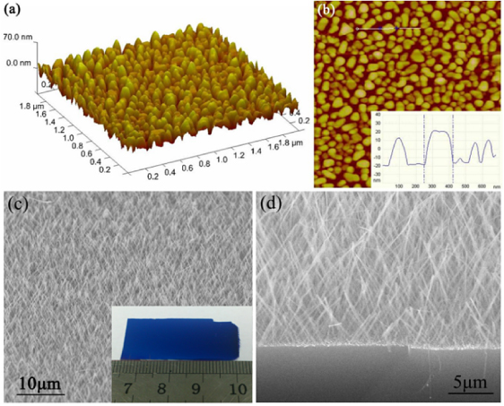
Figure 1. (a), (b) AFM images of the Au NPs on the Si substrate after annealing at 200 ° C for 5 min. The inset in (b) shows the height chart scanned along the white line in (b). (c), (d) ∼30° tilt view SEM images of the large-area CuPc NW array grown on Au-coated Si substrate with different magnifications.
Download figure:
Standard image High-resolution imageTo get a deeper insight into the structural properties of the CuPc NWs, the phase and crystallography of the products were detected by TEM operating at an acceleration voltage of 80 kV. To avoid damage to the NW sample during the transfer process from the substrate to an amorphous carbon-film-coated Cu grid, a thin Si3N4 membrane (thickness 50 nm) coated Si substrate with an opening Si window of 500 μm × 500 μm, which is suitable for TEM examination, was adopted as an alternative. A 6 nm Au seed layer was deposited on the Si3N4 membrane so as to allow the direct growth of the CuPc NW array on it by the same method as that on Si. Figures 2(a) and (b) show a typical TEM images of the CuPc NWs on the Si3N4 membrane. Au NPs are visible at the starting points of the nanowire growth, which is consistent with the SEM observations. HRTEM and SAED show that the CuPc NWs are α-phase single crystalline (figures 2(c)–(e)). The interplanar spacing of 12.5 Å indicates that the NWs have (002) side surfaces, while the growth orientation could be determined to be [010] along the b-axis from the SAED pattern (figure 2(d)). Figure 2(f) illustrates the packing geometry of the CuPc NWs on Au NP [10, 27]. It is noted that the direction of π–π stacking is parallel to the growth direction of the NWs. This is reasonable since π–π stacking is a strong driving force for the 1D anisotropic growth of Pcs.
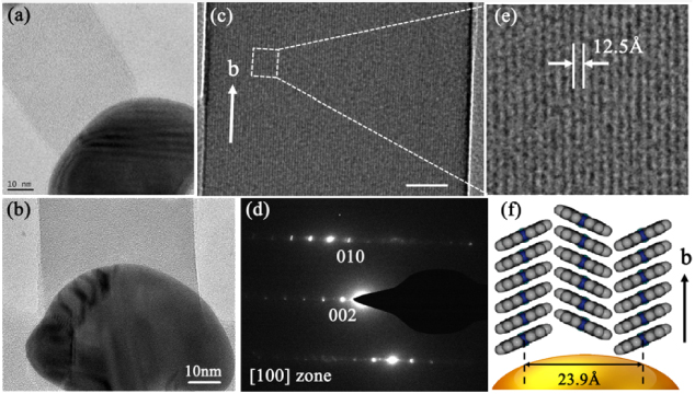
Figure 2. (a), (b) Typical low-resolution TEM images of CuPc NWs grown on Si3N4 membranes; scale bar=10 nm. (c) HRTEM image of a single α-CuPc NW. The arrow indicates the [010] growth direction of the NW; scale bar=20 nm. (d) SAED pattern of the α-CuPc NW. The SAED pattern is indexed for a monoclinic α-CuPc NW down the [100] zone axis. (e) A magnified view of the outlined area in (c). (f) A representation of the crystal structure, which illustrates the molecule arrangement of the NW on Au NPs with π–π stacking parallel to the growth direction.
Download figure:
Standard image High-resolution imageTo verify the crucial role of the Au NPs, in control experiments bare Si wafer without Au film was used for CuPc NW growth. It is noted that no NW arrays could be obtained except for a layer of high density NW film on the Si substrate (supporting information, figure S1 available at stacks.iop.org/Nano/24/355201/mmedia). This result shows that the growth of the CuPc NW arrays is initiated by the Au NPs, which can serve as the active sites for NW nucleation and growth because of their large surface energy. The detailed growth process of the cross-aligned NW arrays was further studied by examining the intermediate products at different time intervals, as shown in figure 3. At the very beginning, just several seconds after the temperature reached the maximum, a layer of Au NPs was formed on the substrate (figure 3(a)). The evaporated CuPc began to selectively nucleate on the high surface energy areas of the Au NPs, and the reaction lasted for about 1 min after reaching the maximum temperature (figure 3(b)). With the progress of the vapor transport, later arriving CuPc molecules would then prefer to grow on the nucleation sites and stack along the π–π direction to form NWs. In contrast to the edge-on orientation on bare Si, CuPc adopted a face-on orientation on Au particles, resulting in the out-of-plane growth of the NWs (figure 3(c)). Eventually, dense and highly aligned NW arrays were obtained after a growth time of about 15 min (figure 3(d)). Figure 3(e) shows a schematic illustration of the growth process for the CuPc NW arrays. Differing from the conventional vapor–solid–liquid (VLS) growth mechanism for most of the inorganic NWs, the substrate temperature (∼180 ° C) was too low to form Au alloy liquid drops during the organic NW growth. Therefore we believe that the Au NPs may simply serve as the active sites for NW nucleation, as well as guide the aligned growth of the NWs. The growth of NWs was probably dominated by a VS process rather than a VLS process [22, 28, 29]. To further clarify whether the alignment was Au template induced or substrate assisted, parallel experiments were conducted. With other conditions kept unchanged, an Au-coated SiO2/Si substrate was used. It is found that the NWs can retain the growth orientation on the SiO2/Si substrate (figures 4(a) and (b)). This observation convincingly proves that the alignment of the NWs is not determined by the nature of the substrate, but by the Au NPs. Moreover, this method can be extended to other organic molecules for their NW arrays growth. Figures 4(c) and (d) show SEM images of PTCDA and copper hexadecafluoro-phthalocyanine (F16CuPc) NW arrays, respectively, prepared by using Au NPs as templates, indicating the good alignment of the organic NW arrays on the substrates.
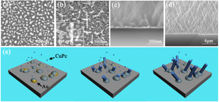
Figure 3. SEM images of the NW array grown at different stages after the evaporation temperature reached 415 ° C: (a) 5 s; (b) 1 min (the inset shows the SEM image at higher magnification; scale bar=100 nm); (c) 3 min; (d) 15 min. (e) Schematic illustration showing the growth process of the CuPc NW arrays.
Download figure:
Standard image High-resolution image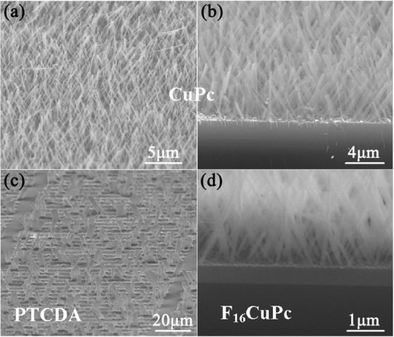
Figure 4. (a), (b) SEM images of CuPc NW arrays grown on the Au-coated SiO2/Si substrate. (c) and (d) SEM images of PTCDA and F16CuPc NW arrays, respectively, fabricated by the Au NP templated method.
Download figure:
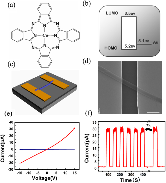
Standard image High-resolution imageFigure 5(a) shows the molecular structure of CuPc. The π–π stacking between the large 2D aromatic planes enables the molecules to self-assemble anisotropically into 1D nano- or microstructures. [10] The high quantum efficiency arising from the single-crystalline nature of the CuPc NW, along with the fast carrier transport along the π–π stacking direction, makes the CuPc NW a promising material for photosensor applications. Recent investigations on inorganic/organic NW-based photodetectors also demonstrated their superior performance because of the size effects and high crystal quality [30, 31]. To assess the photoconductive characteristics of the CuPc NWs, bottom contact devices were constructed based on individual NWs (figures 5(c) and (d)). Cr (5 nm)/Au (50 nm) electrode pairs with an interspace of 8 μm were defined on a SiO2 (300 nm)/p+–Si substrate by photolithography, followed by the dispersion of the as-synthesized CuPc NWs on them via a contact printing method. The work function of the Au electrode is 5.1 eV, which matches well with the highest occupied molecular orbital (HOMO) of CuPc (5.2 eV), thus ensuring a good Ohmic contact between them (figure 5(b)). Figure 5(e) depicts typical current versus voltage (I–V) curves of the device measured in the dark and under red light illumination. The I–V curves are linear and quasi-symmetric, indicating the excellent Ohmic contact of the electrode with the NW. The device exhibits a low conductance in dark with a dark resistance (Rd) as high as 8.3 × 10¹³ Ω. However, a drastic decrease of ∼180 times in light resistance (Rl = 4.7 × 10¹¹ Ω) is revealed, when the light is turned on. Under light illumination, electron–hole pairs were excited and then separated by the external electric field; the drift of the carriers along the NW led to the flow of the photocurrent. The high crystal quality and large surface area-to-volume ratio of the CuPc NW contribute to the large photocurrent as well as the high Ilight/Idark ratio. The photo-switching property of the CuPc NW was further tested by manually turning the laser diode on and off (figure 5(f)). The time response of the device illuminated with pulsed light is fast, highly stable and reproducible. The response time for the device could be deduced to be as low as 100 ms. Significantly, after several tens of cycles and 2 h of continuous operation, no degradation was noted for the unpackaged device operating in ambient air, indicating the high endurance of the device. In comparison with previous reports [32, 33], our devices possess superior performance in terms of higher response sensitivity and faster response speed. This result could be attributed to the intrinsic properties of the CuPc NWs. The NWs were synthesized by PVD in a vacuum and at a relatively high temperature. Therefore they have a higher crystal quality as well as better structure stability than the nanostructures prepared via conventional solution methods. On the other hand, although only single NW-based devices were demonstrated in this work due to the obvious difficulty in fabrication of top electrode on the organic NW array, we believe that CuPc NW array-based devices could be achieved by the means of spin-coating a layer of n-type conductive polymer on the NW array with the formation of a heterojunction structure, using graphene film as the top electrode and so on. Additional experiments are being carried out to fabricate nano-optoelectronic devices based on CuPc NW arrays.
Figure 5. (a) Structure of a CuPc molecule. (b) Highest occupied molecular orbital and lowest unoccupied molecular orbital energy diagrams of CuPc. The Fermi level of Au is also shown for comparison. (c) Schematic diagram and (d) SEM image of the bottom contact device based on an individual CuPc NW; scale bar=5 μm. (e) I–V characteristics of the bottom contact CuPc NW device under dark and light illumination. A red laser diode with a center wavelength of 650 nm, spot diameter of 1 mm and intensity of ∼50 mW cm−2 was used as the light source. (f) The reproducible on/off switching properties of the NW device under the pulsed light illumination. The external bias was fixed at +15 V.
Download figure:
Standard image High-resolution image
4. Conclusions
In summary, we have demonstrated a feasible method for aligned growth of highly dense single-crystalline organic NW arrays by using Au film as a template. The growth process was investigated in detail. Au film was found to serve as the active site for NW nucleation as well as direct the subsequent aligned growth. Photoconductive devices based on the as-prepared single NW demonstrated a pronounced photoresponse to the incident light, with an excellent stability and reproducibility. This strategy shows great potentials for synthesis of organic NW arrays for use in the construction of large-scale high-performance nano-optoelectronic devices.
Acknowledgments
This work was supported by Major Research Plan of the National Natural Science Foundation of China (nos 91027021, 91233110), National Basic Research Program of China (973 Program, grant nos 2013CB933500, 2012CB932400, 2011CB808400, 2010CB934500), National Natural Science Foundation of China (nos 51173124, 51172151). We also thank Natural Science Foundation of Jiangsu Province (no. BK2010003) and a Project Funded by the Priority Academic Program Development of Jiangsu Higher Education Institutions.