Abstract
Stacking thin polymer films supporting metal nanowire gratings provides a simple route, demonstrated here, to producing large-area metallic woodpile structures with high throughput. Under appropriate conditions the grating films can spontaneously roll up, giving a rapid and controllable method of creating multilayers. The resulting three-dimensional (3D) wire structures are flexible and potentially stretchable. Since this process can be extended to include a wide variety of functional materials, it opens up the manufacture of many tailored 3D optical metamaterials.
Export citation and abstract BibTeX RIS

Content from this work may be used under the terms of the Creative Commons Attribution 3.0 licence. Any further distribution of this work must maintain attribution to the author(s) and the title of the work, journal citation and DOI.
This article was made open access on 5 August 2013.
1. Introduction
Metamaterials and photonic crystals are artificial materials that contain a repeating microscopic structure. This gives them unique electromagnetic properties including preventing light propagating within the spectral regions of photonic bandgaps [1], bending light within optical cloaks [2] and overcoming the diffraction limit through negative refractive index superlenses [3–5]. These photonic systems are designed to operate over a specific wavelength range, where the repeating elements must be the size of these wavelengths or less. A metamaterial operating at optical wavelengths requires components that are of the order of 100 nm or less, and hence producing a volume of 1 mm3 would require making 1012 identical components and assembling them accurately. For this reason most such metamaterials have been produced in extremely small volumes, and are mostly derived from thin sheets.
There are currently very few manufacturing techniques capable of producing small structures on a large scale, and some of the currently preferred techniques are illustrated in figures 1(a), (c), (e), (g), (i). Successful implementation of these manufacturing strategies to give photonic band gaps at optical to near-infrared wavelengths are shown in the scanning electron microscopy (SEM) images of figures 1(b), (d), (f), (h), (j). All of these techniques have problems related to low production speed and/or nanofabrication volume, defects, non-manufacturability and inherent cost of scale-up. We briefly review a few of these before presenting a new approach which we have successfully shown can be applied to creating such metamaterials.

Figure 1. (a), (c), (e), (g), (i) Summary of current techniques to manufacture photonic crystals with corresponding SEM images of typical fabricated structures alongside (b), (d), (f), (h), (j), reproduced from [6, 8–11] respectively. The techniques are (a), (b) self-assembly of colloidal particles, (c), (d) direct laser writing, (e), (f) electron beam lithography and micromanipulation, (g), (h) reactive ion etching through a mask and (i), (j) interference holography. (k) Schematic for a new technique of stacking wire gratings presented in this paper and (l) SEM image of a self-rolled thin film wire grating. Images in (b), (d), (f), (h), and (j) are reproduced with permission from, respectively, [6] copyright Royal Society of Chemistry 2010; [8] copyright John Wiley and Sons 2012; [9] copyright Nature Publishing Group 2010; [10] copyright John Wiley and Sons 2012; and [11] copyright The Optical Society 2006 .
Download figure:
Standard image High-resolution imageThe honeycomb periodic structure of figure 1(b) is formed by the self-assembly of microspheres into a lattice (figure 1(a)). This template is then infiltrated with silica and the spheres dissolved to leave the inverse silica crystal behind [6]. This is an efficient and inexpensive manufacturing process however there is very little control over the resulting crystal structure, which critically affects the optical response.
Woodpile structures (figures 1(d), (f), (h), (j)) have a favoured morphology for broad bandwidth and complete photonic bandgaps. Much current interest in this structure also arises because it can be manufactured simply by stacking layers of rods or wires, with each layer orientated perpendicular to the previous one. If the rods are stacked to produce a face-centred cubic lattice (figure 1(c)) the woodpile has a diamond-like crystal structure which has been shown to produce robust and often complete photonic band gaps [7].
The woodpile structures of figures 1(d) and (f) are fabricated respectively by direct laser writing [8] and by electron beam lithography followed by stacking through micromanipulation [9] (figures 1(c) and (e)). Each of these methods is expensive and time-consuming and produces structures that are very limited in their overall volume. There is also an inherent inefficiency in drawing out a woodpile repeatedly line by line. A method where many lines can be created at once would be a highly preferable fabrication strategy.
One of the major hurdles when fabricating woodpile structures is the alignment of the rods in neighbouring layers with the same orientation. Careful alignment is necessary to create a periodicity in the direction normal to the wire layers. For example each layer used to build the woodpile in figure 1(f) has notches that slot into three alignment posts, resulting in a formidably slow assembly process.
Inverse-woodpile photonic crystals can also be produced (figures 1(g) and (h)) by etching cylindrical pores through the material, instead of assembling a lattice of solid rods. The pores here are etched into two orthogonal silicon surfaces using optimized reactive ion etch techniques through a photolithographic mask [10]. Again careful alignment is needed during the second etch to ensure that a diamond-like lattice is formed. This method is efficient in that it creates many pores with one processing step, however the pores only penetrate 5 μm into the silicon which severely limits the overall size of the metamaterial created. The reactive ion etching processes are also expensive and require careful optimization [10]. Energy loss with depth is also a major limitation for interference holography (figures 1(i) and (j)). In this technique multiple laser beams interfere with each other to produce a woodpile structure in one shot with automatic periodicity in three dimensions [11], but that is restricted in overall thickness by absorption and scattering.
Here, we introduce and demonstrate the feasibility of an alternative approach for manufacturing woodpile structures that is inexpensive, efficient and can produce nanostructures over arbitrarily large areas. The woodpile structure is constructed by stacking thin textured polymer films that have been patterned with metal nanowire arrays. The wires form the rods of the woodpile and provide a permittivity contrast with the surrounding polymer similar to that in semiconductor woodpile photonic crystals exhibiting full photonic band gaps [12, 13]. This method makes use of the ability to capture thin polymer films on a water surface, where they can be handled and manipulated [14]. We construct ultrathin self-supporting patterned layers that are then stacked or rolled into the desired 3D geometries. Our process can be extended in a large variety of ways, for instance incorporating non-metallic, metallic, magnetic or active photonic materials into the woodpiles for future large-scale devices.
The proposed method is illustrated schematically in figure 1(k). Initially two films forming the woodpile basis are stacked one on top of the other so that the two wire gratings are mutually perpendicular. This bilayer can then be either rolled up (figure 1(l)), folded or cut and stacked [14–16] to build the 3D woodpile photonic crystal. The films are flexible enough for their textures to be transferred through multiple layers, hence during the stacking of the textured bilayer film, the wires in neighbouring bilayers are able to automatically align as textures of the two films lock together, harnessing self-alignment for large scale nanoassembly. Because all layers throughout the photonic crystal arise from a single fabricated bilayer, their uniformity is far easier to control than with successive depositions or etch steps. The resulting metal–polymer metamaterial is flexible and deformable, and so can be used in arbitrarily curved geometries unlike conventional hard photonic crystals, and can be elastically tuned.
To demonstrate the feasibility of the method, polystyrene films of sub-micron thickness supporting gold wire gratings of periodicities 278, 417 and 556 nm have been successfully fabricated over large areas. Bilayers of crossed wire gratings that form the woodpile basis layers have then been produced, and their first assembly and optical response is reported.
Further, a very promising new assembly technique is demonstrated whereby thin film wire gratings self-roll into multilayers, producing rolls with diameters down to 10 μm. Metallic micro-helices could be produced by choosing the rolling direction relative to the wire orientation providing a new route to fabricating chiral metamaterials that can exhibit a negative index of refraction in the near and mid-infrared [17–19]. Different chiralities should lead to different optical responses in analogy with carbon nanotubes.
2. Experimental section
We use an imprint method to form the stackable metal wire arrays (figure 2). In summary, gratings are imprinted into a soft sacrificial layer, onto which metal is deposited at a steep angle transverse to the grating lines, creating wires that span the length of the sample. The wires are then coated in a thin (150 nm) polymer film and the underlying sacrificial layer is dissolved leaving the wires attached to the underside of the polymer film, which floats on the surface of the solvent. To create a woodpile structure, the floating thin film wire grating can then be deposited onto another grating orientated perpendicularly to it, resulting in a polymer bilayer with two crossed metal gratings separated by the polymer film thickness. This bilayer can then similarly be released onto a liquid surface from which it can be stacked or folded or rolled up to form the desired photonic crystal structure [15].

Figure 2. Schematic of thin film wire grating manufacture, for fabricating woodpile photonic crystals. A polystyrene sulfonic acid (PSS) film is spin-coated onto a Si substrate (a), imprinted with a fluoropolymer (ETFE) grating (b), and coated with Au wires by glancing angle evaporation (c). Another polymer film is then spin-coated on top (d), the PSS layer is dissolved in water to release the wire grating polymer film (e) which is then collected onto the structure from step (d) with the grating orientated perpendicularly (f). Again the PSS layer is dissolved in water to release the bilayer gratings (g) which can be stacked as desired to produce a woodpile structure (h).
Download figure:
Standard image High-resolution imageThe grating nanostructure that underpins this method can be produced in several ways including using deep-etched silicon master gratings or using direct interference lithography. Here we show results for silicon diffraction gratings which are readily available (LightSmyth Technologies) with variable pitch and 140 nm deep grooves. The rectangular profile of one such grating is recorded with tapping mode atomic force microscopy (AFM) (figure 3(a)) showing the steep edges convolved with the AFM tip angle. The cm2 areas of these master gratings currently limits the area of structures produced, however this can be scaled up by incorporating the grating embossing in a cylinder imprint printing process.

Figure 3. (a) AFM profiles of an inverted master silicon grating (solid dark grey), an intermediate ETFE grating (black dashed line) and an ETFE-imprinted PSS film (solid light grey), each with grating period 556 nm. (b) SEM image of an evaporated Au wire grating on an imprinted PSS grating with period 278 nm. (c), (d) Photograph of a Au wire grating on a polystyrene film (area 1 cm2, thickness 300 nm, grating period 417 nm) deposited on a Si substrate, with (c) and without (d) diffracted light from the grating region illuminated by a white lamp.
Download figure:
Standard image High-resolution imageTo increase the life of the silicon gratings and to make the imprinting process more robust, the master gratings were transfer moulded into a stiff yet flexible fluoropolymer of ethylene tetrafluoroethylene (ETFE) [20]. Imprinting with a flexible material allows for greater control when separating the two surfaces after the imprint, since it can be bent. The fluorinated surface of the ETFE also inhibits the transfer of material from one surface to another during the imprint process.
Nanoimprints were performed in an Obducat nanoimprinter which provides temperature and pressure control with a uniform pressure over the imprint area. The resulting AFM surface profiles (figure 3(a), dashed line) indicate that the imprinted ETFE grating keeps 100% of the master grating depth, but some definition is lost at the corners.
The ETFE grating moulds are then used to make thin polymer films patterned with metal wire gratings using the initial steps outlined in figures 2(a)–(e). Initially a 1 μm-thick film of polystyrene sulfonic acid (PSS) is spin-cast onto a silicon substrate (figure 2(a)). This film plays two roles in the manufacturing process; firstly it is the material that is imprinted with a grating profile onto which the metal wires are deposited, requiring it to be soft but non-elastic, and secondly it is a sacrificial layer that allows the wires to be released from the substrate. The polymer PSS is chosen as the sacrificial layer because it is highly soluble in water, which is an ideal solvent due to both its easy handling and its high surface tension which supports sub-micron polymer films on its surface completely flatly. Gratings are imprinted from ETFE moulds into the PSS film (figure 2(b)) at a temperature of 150 ° C and pressure of 20 bar. The AFM profile of the resulting PSS surface (figure 3(a)) retains 100% of the ETFE grating depth, but exhibits a slight loss of edge definition.
Gold is then deposited by electron beam evaporation at a glancing angle onto the PSS surface grating (figure 2(c)). Deposition parameters used were 0.05 nm s−1 for 400 s at an angle of 80° to the surface normal. A typical resulting array of gold wires using these parameters (figure 3(b)) shows a period of 278 nm and Au line widths of 70 nm. The periodicity of the wires is determined by the imprinted grating period and their shape can be varied with the angle and deposition time. The Au thickness is estimated from cross-sectional images to be between 20 and 40 nm.
The next fabrication step is to deposit a polymer film on top of the gold wire/PSS composite (figure 2(d)), by spin-coating a polystyrene solution. To obtain the desired photonic crystal periodicity once the film is stacked up, the film thickness is measured with ellipsometry and is carefully controlled by varying the polymer concentration and spin speed. In the present case we require thicknesses of around one quarter of the target wavelength inside the medium, so ∼150 nm. In principle the film can be made from any polymer, providing that its solvent does not dissolve the underlying PSS.
The polystyrene film is then released from the substrate by dissolving the PSS layer underneath it in water such that the film is captured onto the water meniscus. We utilize a scheme in which the sample is angled at 45° into a controlled water bath, resulting in a progressively advancing wetting line on the sample surface, which allows the film to detach directly onto the water surface. As the PSS dissolves, the gold wires fully adhere to the bottom of the polystyrene film (figure 2(e)). The floating polystyrene film with the gold wire grating on its underside can then be collected onto the desired substrate in any orientation, or onto other thin film wire gratings for subsequent stacking. After deposition a layer of water temporarily remains between the film and substrate, during which time fine adjustments of the film alignment can be made before the water evaporates.
The photographs in figures 3(c) and (d) show such a thin film wire grating collected onto a silicon substrate from below the water surface. The high quality of the grating transferred from the silicon master to the polystyrene film, despite having undergone multiple imprints into ETFE and PSS, is evident from the uniform green diffraction colouration (figure 3(c)) across the entire film (1 cm2). The polystyrene film itself is also high quality and deposits flatly onto the substrate with no cracks or wrinkles (figure 3(d)).
Multi-directional stacks of thin film wire gratings may be constructed using this method of floating and collecting, with customizable grating orientations. Preliminary results of perpendicular bilayer grating stacks are presented in section 3.
3. Results and discussion
3.1. Stacking of multilayer wire gratings
The success of the fabrication technique can be observed in the images of the individual grating layers, and their multiple stacking and assembly (figure 4). The successful transfer of gold wire gratings onto polystyrene films is evident with SEM imaging (figure 4(a)).

Figure 4. SEM images of stacked polystyrene (PS) films with wire gratings. (a) Distinct Au wires on a polystyrene film are visible at the torn film edge. (b) Two films stacked with perpendicular grating directions. (c) Cross-section of a double bilayer stacked by rolling onto a glass rod. Perpendicular grating wires are indicated with red and blue lines.
Download figure:
Standard image High-resolution imageTo form a woodpile structure, a bilayer of two thin film wire gratings with orthogonal orientations is assembled and then released as one film to be rolled, folded or stacked. The basis bilayer can be constructed by collecting a thin film wire grating from a water surface onto a similar film still on its initial substrate and PSS layer (figure 2(f)), allowing release of the bilayer at a later stage to form the woodpile structure (figures 2(g) and (h)). In order to have a polystyrene layer separating the two wire gratings, as in the desired woodpile structure, the floating film must be collected from below the water surface, making it essential for the water-soluble PSS layer on the substrate to be completely sealed by polystyrene so that it is not dissolved when the sample is immersed. The successful assembly and stacking of such bilayer films can be observed in films which have been slightly peeled apart at their edges (figures 4(b) and (c)) in order to allow electron microscopy.
3.2. Optical response of single and bilayer thin film gratings
To verify the effective production of these flexible nanowire arrays and their uniformity, which is crucial for metamaterials, we measure the single layer and bilayer optical reflectivity.
The specular reflectivity spectrum of the thin film gold wire gratings is measured for incident angles from normal incidence 0° to 60° using an automated goniometer system. The samples are illuminated by a super-continuum white light laser and spectra are collected using a combination of visible and infrared spectrometers. An ultra-broadband Glan–Thompson polarizing cube placed in the beam path before the sample allows illumination with either transverse (electric field perpendicular to the length of the wires) or longitudinal polarization.
The reflection from a thin film gold wire grating with an imprinted period of 278 nm is shown in figures 5(a) and (b), for the two different polarizations. The wire grating is sandwiched between a 330 nm thick polystyrene film and a silicon substrate, with the length of the wires orientated along the goniometer axis of rotation to probe diffractive modes. The data in figures 5(a) and (b) shows a variety of optical effects. The broad fringes are Fabry–Perot modes caused by interference between light reflected at the top and bottom surfaces of the polystyrene film, and match transfer matrix simulations of unpatterned films without gratings rather well (figures 5(c) and (d)).
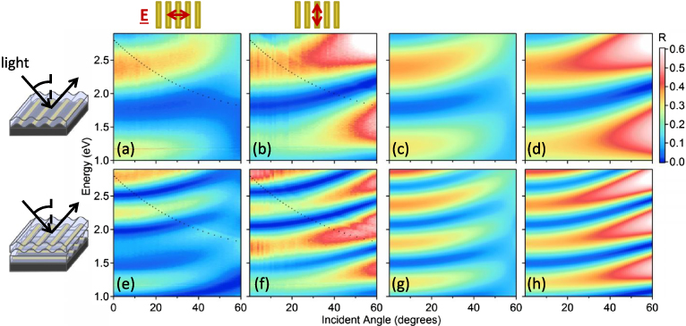
Figure 5. (a), (b), (e), (f) Measured reflectivity dispersions normalized to a silver mirror for (a), (b) single 278 nm periodicity Au wire grating polystyrene films on Si and (e), (f) bilayers of the same film with gratings orientated perpendicularly for transverse (a), (e) and longitudinal (b), (f) incident polarizations. The calculated lowest order Wood's anomaly mode (260 nm periodicity, refractive index 1.59) is represented by black dotted lines. (c), (d), (g), (h) Simulated reflectivity dispersions from the transfer matrix method of unpatterned polystyrene films on Si substrates with thicknesses 330 nm (c), (d) and 660 nm (g), (h) for transverse magnetic (c), (g) and transverse electric (d), (h) polarizations.
Download figure:
Standard image High-resolution imageThe data taken with longitudinal polarization (figure 5(b)) also contains a fainter, sharper mode in the upper right corner of the image, which is tracked by the superimposed black dotted line. This corresponds to the lowest order Wood's anomaly mode for the wire grating [21, 22]. These modes occur when a given wavelength is diffracted into the plane of the grating, which can be calculated by solving |kout∥|2 = |kin∥+Gn|2 where kout∥ = kout. Here kout is the wavevector of the diffracted light with an in-plane component of kout∥,kin∥ is the in-plane component of the incident light and Gn = na* is a reciprocal lattice vector of the grating. The black dotted line overlaid onto each data plot in figures 5(a), (b), (e), (f) is the lowest order solution to this equation for a grating of period 260 nm in a refractive index of 1.59, corresponding to that of polystyrene. The measured mode does not exactly fit the calculated mode for several possible reasons including slight misalignments of the grating in the spectroscopic measurements or the slight deformation and wrinkling of the film when deposited onto the substrate, causing variations in the grating period.
The lower images (figures 5(e) and (f)) show the reflection from a bilayer of two thin film gold wire gratings, identical to those described above, stacked on top of each other so that the gratings are perpendicular to each other. The bilayer is orientated with the wires of the uppermost film parallel to the goniometer rotation axis. The Fabry–Perot modes have doubled in frequency as expected from the doubling of the total polystyrene film thickness (figures 5(g) and (h)), and the Wood's anomaly mode is clearly present for both polarizations as there are now grating lines both transverse and longitudinal to the electric field in each polarization. We also note the splitting of the grating modes in the longitudinal polarization (figure 5(f)), which we believe is due to second order grating coupling.
Silver gratings may also be fabricated using an identical technique, and these are more suited to visible wavelength metamaterials due to the blue-shifted plasmonic resonances. Further work is under way to fabricate and characterize such silver grating multilayers.
3.3. Self-assembled multilayers via directed release-rollup
While sequential stacking or folding is one route to obtaining 3D metallic photonic crystals from these bilayers, an efficient method for obtaining multiple layers of these thin film wire gratings is to take a single film and roll it up (figure 6(a)). This nanofilm roll-up can happen spontaneously under selected conditions [23]. The images in figures 6(b)–(d) show a 300 nm thick polystyrene film supporting a 556 nm period gold wire grating that has formed a roll 1 cm in length after being immersed in water. The gold wires are orientated along the roll length and cover the outer surface of the roll (figure 6(d)).

Figure 6. (a) Schematic of directed self-rolling of thin film wire gratings: sample is partially immersed in water, film rolls from bottom edge up to water surface, sample is further immersed in water, film continues to roll up to higher water surface. (b)–(d) Optical images of rolled-up film with increasing magnification showing (b) entire 1 cm roll length, (c) quality of roll and (d) wire grating on roll surface. (e) SEM image of self-rolled thin film grating.
Download figure:
Standard image High-resolution image
A key parameter that determines whether or not the film will roll up is the hydrophilicity of the film's top surface. If it is hydrophilic then water prefers to wet its top surface so that the entire film becomes immersed, however if it is hydrophobic then water prefers to stay underneath the film allowing the film to be captured on the meniscus by surface tension, preventing roll up. The hydrophobic polystyrene on the top surface of a thin film grating sample must therefore be briefly etched with oxygen plasma to render it hydrophilic. When the sample is now immersed in water, the surface of the film wets allowing roll up to initiate as the PSS dissolves.
The rolling mechanism (figure 6(a)) starts when the bottom of the sample wets in water and the PSS layer underneath begins to dissolve from the edges inwards. As the bottom edge of the grating film is released from the substrate it curls upwards, and as the PSS dissolves further the film continues to curl forming a roll. The film keeps rolling up until all of the PSS that is below the water surface has dissolved. If the sample is moved further into the water the film continues to roll up as more PSS dissolves. The sample can then be removed from the water and the film remains rolled up. The roll of 3D metallo-dielectric film shown in figures 6(b)–(d) has over twenty layers, limited only by the length of the initial film. The roll has an approximately spiral cross-section, with a minimum diameter of around 25 μm and a maximum diameter varying between 100 and 200 μm. The diameter can be controlled as in related roll up of nanoscale films [23–27]. These diameters are large relative to the periodicity of the grating lattice, so different strains between layers do not affect the structure.
The driving mechanism behind the observed self-rolling is here likely the strain built up on the bottom of the polystyrene film, causing the underside of the film to expand when released from the substrate. This can be controlled in a number of ways including by solvent swelling, ultraviolet (UV) cross-linking and other techniques [24–27]. This phenomenon of self-rolling can be harnessed to easily fabricate large-scale grating multilayers. By increasing the driving strain and the length of film that is rolled up, it should be possible to create rolls with hundreds of grating layers, as we have recently achieved with planar roll up. Such metamaterial tubes would allow optical measurement of a many layered structure and could potentially be used as hollow waveguides, filters for sub-wavelength imaging [5] or textured microfluidic channels [25].
Roll diameters on the micron scale have also been produced, as shown in figure 6(e) where a tight roll with 10 μm diameter has spontaneously self-assembled at a film edge. Excellent groove coalignment in angular orientation is evident and further measurements are under way to quantify the degree and uniformity of this alignment. The direction of roll up relative to the orientation of the grating can be controlled by defining the area of film released from the substrate and the angle of the advancing water meniscus. Hence helical wire structures can be formed with a chosen chirality in analogy with carbon nanotubes, providing a route towards chiral metamaterials with a customizable optical response in the visible and near to mid-infrared.
4. Conclusions
We have presented a new, rapid and inexpensive method to fabricate woodpile 3D metallo-dielectric photonic crystals that operate at optical wavelengths, are flexible and have areas of several cm2. Our method involves stacking thin polymer films patterned with gratings of metal wires that are created by glancing angle deposition onto an imprinted diffraction grating. By capturing these films on a water surface the gratings can be stacked or rolled up as desired.
To demonstrate the feasibility of our method, polystyrene bilayers containing two-dimensional gold wire grids with a periodicity as small as 278 nm have been fabricated, stacked and characterized. Polystyrene films patterned with a single gold wire grating have been shown to roll up spontaneously under appropriate conditions when released from a substrate, demonstrating the promise of these manufacturing techniques as a route towards scalable nanofabrication.
Acknowledgments
This work was funded by UK EPSRC Grant EP/G060649/1 and ERC grant 320503 LINASS. We acknowledge Nokia Research Centre Cambridge for the use of their atomic force microscope and Dr Ventsi Valev for helpful suggestions.