
Abstract
We demonstrate an advanced fabrication method for perfectly position-controlled ferromagnetic semiconductor (Fe,Zn)3O4 nanodot arrays down to several hundred nanometers in size surrounded by a ferroelectric BiFeO3 matrix. By performing position-selective crystal growth of perovskite BiFeO3 on the position-controlled epitaxial spinel (Fe,Zn)3O4 nanodot-seeding template, which is prepared using a hollow molybdenum mask lift-off nanoimprint lithography process on a perovskite La-doped SrTiO3(001) substrate, we produce functional oxide three-dimensional lateral heterojunctions. The position-selectivity can be explained based on standard surface diffusion theory with a critical nucleation point. Establishing this fabrication process could lead to innovative nanointegration techniques for spintronic oxide materials.
Export citation and abstract BibTeX RIS
1. Introduction
Periodic nanostructures surrounded by a matrix of another material have considerable potential for use in a variety of innovative nanodevice applications because of the introduction of original spin and/or electronic couplings generated by newly constituted lateral interfaces between the two phases. These lateral heterojunctions offer the possibility of creating vertical magnetic field-effect transistors to control magnetic and electric properties through the interfaces by using an electric field [1–5], leading to advanced spintronic devices such as ultra-high density data storage devices using charge and spin degrees of freedom. In particular, a combination of magnetic semiconducting oxides [6, 7] and ferroelectric oxides holds promise for fabrication of a device that work at room temperature [3–5]. Fabrication of this type of nanostructure, however, is still challenging and remains a developing process. Self-assembly synthesis has generally been used to fabricate such nanodot and nanopillar arrays, embedded in a matrix of functional oxide materials [8–13] as a convenient bottom-up fabrication method. However, precise control of the spatial positioning, structural shapes and sizes of the nanostructures remains a difficult problem, although a number of nanocomposite structures can be fabricated over a large area. Template-assisted selective growth [14] and masked patterning [15] techniques hold considerable potential to control the positioning of nanoheterostructures. A suitable method to satisfy the precise alignment requirements of these devices would be the use of nanotemplates. In this paper, we demonstrate an advanced fabrication method combined with top-down nanoprocessing based on nanoimprint lithography and a bottom-up nanoprocess based on self-selective crystal growth on the template, and offer lateral heterojunctions with perfectly position-controlled ferromagnetic nanodot arrays surrounded by a ferroelectric matrix. This method overcomes the issues of precise position, size and shape control. The nanoimprint lithography method on which we have focused includes a promising top-down nanotechnology process to produce a template with perfect position, shape and size control of the nanostructure arrays over a large area. We have experimentally demonstrated our original fabrication technique for precisely position-controlled magnetic oxide nanodot arrays as small as 60 nm in a millimeter-sized area [16]. The oxide materials selected for this research are spinel Fe2.5Zn0.5O4 (FZO) with ferromagnetic semiconducting properties [6] and perovskite BiFeO3 (BFO) with ferroelectric properties, with the aiming of creating innovative nanospintronic devices such as magnetic field-effect transistors [1–5].
2. Experimental details
The perfectly positioned FZO nanodot arrays were prepared using a combination of ultra-violet nanoimprint lithography, pulsed laser deposition (PLD) and hollow metal molybdenum (Mo) lift-off mask techniques. The detailed fabrication process has already been reported in [16]. The nanodot FZO arrays on a La-doped SrTiO3(001) (La-STO(001)) substrate act as a fine seeding template for self-assembly growth of perovskite BFO. We investigated the self-selective growth conditions of BFO as a function of various sizes of the FZO nanodots. BFO was deposited by a PLD technique with appropriately set conditions of oxygen pressure of 10 Pa and a substrate temperature of 650 °C to obtain crystallized BFO thin films. Figure 1 shows the XRD results of 2theta/theta measurements using the Cu Kα line (λ = 1.5405 Å) for the bare STO(001) substrate and the results after BFO deposition on the FZO nanodot substrate. The peaks can be attributed to spinel FZO (00l) and perovskite BFO (00l) based on the lattice constants of spinel FZO (a = b = c = 0.847 nm) [7] and of perovskite BFO (a = b = 0.394 nm, c = 0.400 nm) [17], respectively, without any other phases.

Figure 1. Results of 2theta/theta measurements from XRD of the sample after BFO deposition on a ZFO-dot seeding SrTiO3(001) substrate (blue curve) and a bare SrTiO3(001) substrate (black curve).
Download figure:
Standard image3. Results and discussion
Figure 2 shows SEM images of FZO nanodot arrays after BFO deposition on the seeding substrates with dot sizes of (a) 3 μm, (b) 800 nm, (c) 500 nm and (d) 100 nm on a side. Well-positioned FZO nanodot arrays are observed across the whole area, as already shown in [16]. As shown in the magnified images of the FZO dot in the insets of figures (a)–(d), segregated grains appear on the FZO terraces of 3 μm-sized dots, while there are no segregation phases for dot sizes below 800 nm. To clarify the spatial distribution of each element in detail, we performed elemental mapping measurement using an electron probe microanalyser. Figure 3 shows the elemental mappings of Bi and Zn atoms on the samples with 800 nm sized FZO dots. The Zn-rich region is on the dots only, while the Bi-rich region is on the matrix. Figures 4(a)–(d) show atomic force microscopy (AFM) images of 3 μm and 500 nm FZO dots before and after BFO deposition. Before BFO deposition, the terraces of the FZO dots are clearly flat, as shown in the images of figures 4(a) and (c) and the cross-section profiles of (e) and (f). After BFO deposition, on the other hand, nanosized grains derived from the ablation of BFO targets nucleated on the terraces of 3 μm-sized FZO dots, while the flat surfaces are maintained on the terraces of the 500 nm sized FZO dots even after BFO deposition, as seen in figures 4(d) and (f). Also, the thickness on the terraces of 500 nm sized FZO dots remains unchanged after deposition while the thickness on bare La-STO(001) substrates increases after BFO deposition as shown in figure 4(f).

Figure 2. SEM images of the samples of (a) 3 μm dots, (b) 800 nm dots, (c) 500 nm dots and (d) 100 nm dots of FZO, respectively, embedded in a BFO matrix. The insets show magnified FZO dots.
Download figure:
Standard image
Figure 3. EPMA mappings of (a) Bi atoms and (b) Zn atoms in the sample with 800 nm sized FZO dots.
Download figure:
Standard image
Figure 4. AFM images before BFO deposition on the samples with (a) 3 μm- and (c) 500 nm sized FZO dots and after BFO deposition on the samples with (b) 3 μm- and (d) 500 nm sized FZO dots. The cross-section profiles before (L1 and L3) and after (L2 and L4) BFO deposition on the samples with (e) 3μm- and (f) 500 nm sized FZO dots.
Download figure:
Standard imageFollowing our assessment of this series of evaluations, BFO is selectively grown on a La-STO(001) surface, avoiding FZO dots with smaller dot sizes of less than 800 nm in our experiments.
The dependences of the selective crystal growth of BFO and the FZO terrace size can be explained using standard surface diffusion theory. When F is the spatially homogeneous atomic or molecular flux arriving at the surface from the ablation of a BFO target, the diffusion equation expressed as a function of the density of adatoms C(x) is

where DS is the diffusion coefficient.
In the steady-state, i.e.  , equation (1) can be represented in the one-dimensional case as follows:
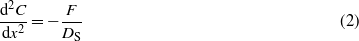
According to Shitara et al [18], adatoms are absorbed into the edges. Therefore, as a boundary condition, there are no adatoms on the terrace terminals at x = 0 and l, as shown in the schematics of figure 5(a), i.e. C(0) = C(l) = 0. This boundary condition is important for nucleus growth, depending on the terrace width l. Finally, we obtained the following quadric equation:

F is a fixed parameter in this experiment because the supply and supplemental speed of the ablated molecules from a BFO target remain constant for each sample, which requires the same ablation time, laser energy and laser frequency. The DS value is dependent on the surface energy of FZO and BFO and on the interface energy between FZO and BFO, and has a constant value in this experiment. The maximum value of C(x) becomes Cmax = Fl2/8DS at the middle of the terrace (x = l/2), represented by the parabolic dot lines following equation (3) in figure 5. In the nucleation model, when the maximum value goes beyond the critical threshold C0, i.e. Cmax > C0, the adatoms coalesce and nucleation emerges in the supra-threshold area, as shown in the left schematic of figure 5. The width of the nucleation area W as a function of l derived from  can be represented as
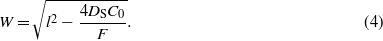

Figure 5. Model based on the surface diffusion theory of adatoms to explain position-selective growth of BFO. The schematic illustrations show the imperfect (the left panel) and perfect (the right panel) selective growth according to the ZFO terrace width (l or l'). The parabolic curves show the spatial density of adatoms C(x) following equation (3) during BFO deposition. The critical nucleation threshold C0 is independent of the terrace width.
Download figure:
Standard imageThe point of the nucleus growth on the terrace is where W is a real number in equation (4). In the case where  , nucleation appears, while in the case where
  , perfectly selective growth then occurs. Thus, a small l value tends to lead to perfectly selective growth, as shown in the right schematic of figure 5. This scenario can qualitatively explain the experimental results.
Finally, we investigated the electronic properties of local points using conductive atomic force microscopy (C-AFM). Figure 6(a) shows the bias voltage dependence of the current curve on each local point of the La-STO substrate, the FZO and the BFO in the sample of 800 nm sized FZO dots that were measured by C-AFM; the curves for FZO and BFO show nonlinear semiconducting and insulating behavior, indicating fine properties as a semiconducting channel and a gate insulator, respectively, while that for La-STO shows fine metallic behavior as an electrode. In nanoscaled electronic mapping, a spatially homogeneous current image is clearly observed on the FZO terrace, while the current is prevented on the BFO matrix, as shown in figure 6(c), compared with the coincidentally measured topography shown in figure 6(b). With regard to the magnetic properties of the FZO dots, ferromagnetic characteristics are shown in the magnetic force microscopy images of figures 7(a) and (b). The magnetization inversion can be clearly observed. From these results, the BFO matrix and the FZO dots are seen to be capable of forming a gate insulator with spatially homogeneous electronic properties and a magnetic channel, respectively.

Figure 6. (a) Bias voltage dependence of current measured on local points of an FZO dot (red dots), a BFO matrix (blue dots) and the La-STO bottom electrode substrate (black dots). (b) A topographic image and (c) a current image at bias voltage of 0.2 V in the sample with 800 nm FZO dots.
Download figure:
Standard image
Figure 7. Magnetic force microscopic images after (a) applying magnetic field to the sample with 400 nm FZO dots and (b) applying inverse magnetic field.
Download figure:
Standard image4. Conclusions
In summary, this research demonstrated an advanced fabrication method for the preparation of three-dimensional oxide heterojunctions based on FZO dots and a BFO matrix in a wide region of 9 × 9 mm2 by combining nanoimprint lithography and self-selective crystal growth. The results showed that the fully aligned epitaxial semiconductive–ferromagnetic FZO nanodots were perfectly surrounded by an insulating BFO matrix below the critical terrace width for nucleation lC by taking advantage of self-assembled crystal growth. This fabrication technique can resolve the precise position alignment issue for nanoheterostructures, which will be widely available for other material combinations [19] and will be useful for high density nanointegration of spintronic devices in the future. Our achievement here may lead to the advanced integration of heterojunctions composed of oxide materials with precise position, size and shape controllability over a large area.
Acknowledgments
The authors thank T Tanaka (Comprehensive Analysis Center ISIR, Osaka University) and M Sakuma for their experimental assistance. This work was supported by a Grant-in-Aid for Scientific Research on Innovative Areas (No. 23104507) from the Ministry of Education, Culture, Sports, Science and Technology, Japan.