
Abstract
The reliable fabrication of nanoelectrode pairs with predefined separations in the few nanometer range is an essential prerequisite for future nanoelectronic devices. Here we demonstrate a fine-tuned electron-beam lithographic (EBL) fabrication route which is suitable for defining nanoelectrode pairs with a gap size down to 3 ± 1 nm and with a yield of 55%. This achievement is based on an optimized two-layer resist system in combination with an adopted developer system, as well as on an elaborated nanoelectrode pattern design taking into consideration the EBL inherent proximity effect. Thus, even a structural control in the nanometer scale is achieved in the EBL process.
Export citation and abstract BibTeX RIS
1. Introduction
The emerging field of nanoelectronics and nanophotonics requires patterns with dimensions smaller than 100 nm for the integration of nanomaterials. In particular, a further reduction of feature size is demanded to enable the future integration of nanoscale objects with tailored functionalities, such as carbon nanotubes, nanoparticles or even single molecules. So far, several methods exist in the laboratory to connect reliably nanoparticles or molecules to the macroscopic outer world [1], such as scanning probe microscopy, break junctions, hanging mercury drop junctions or nanopores. Furthermore, individual nanoelectrodes can also be produced successfully by more sophisticated methods such as: gold plating [2], nanosculpting by application of a transmission electron microscope (TEM) [3] or a focused ion beam FIB [4], as well as self-alignment techniques [5, 6], electromigration [7, 8] or an additional metallization step [9]. However, advanced lithographic techniques seem to be most suitable to meet the demand to fabricate larger numbers of contacts to nanoscale objects.
Advanced lithographic methods for the direct patterning of nanometer-scaled devices on large or medium areas are: extreme UV lithography (EUV), nanoimprint lithography (NIL) or e-beam lithography (EBL) [10, 11]. EBL is a suitable technique to create ultra-small structures, such as sub-20 nm lines or nanoelectrode pairs with separations smaller than 30 nm [9, 12, 13]. The process is based on direct writing with a focused electron beam in a resist layer to achieve the respective nanostructures. Thereby the structural control is limited by the fabrication process itself, i.e. the homogeneity and stability of the resist film, the roughness of the evaporated metal film, the development process and problems due to the scattering of electrons (the proximity effect). The standard resist for very high resolution EBL is PMMA (polymethyl-methacrylate). Nanoelectrode structures are fabricated advantageously with a double resist layer stack of PMMA–MAA (polymethyl-methacrylate with 33% methacrylic acid, undercut layer) and PMMA (mask layer). However, for sub-30 nm electrode separations a limited reproducibility is observed due to the instability of the mask layer in this process [13].
The proximity effect related exposure in EBL is a consequence of electron scattering due to their interactions with each other and with atoms in the resist and substrate. This parasitic exposure of an unwritten area due to both forward and backward scattered electrons in the exposure beam limits the resolution of the resist-developer system. The forward scattering is caused by Coulomb interactions between electrons within the beam leading to a spread of the electron beam to a Gaussian dose profile. This beam broadening up to 10 nm depends on the acceleration voltage, the resist material and the resist thickness. Back scattering of the incident electrons occurs mainly due to interactions with the atoms in the substrate. The intensity of these backscattered electrons depends on the acceleration voltage and the substrate material. The consequence is an exposure of the resist for the second time over a large area with a radius of tens of µm around the incident electron beam. A correction of this proximity effect related exposure can be performed with the commercially available program PROXECCO. However, this method significantly fails to correct features below 65 nm accurately [14]. Here we will show the fabrication of sub-5 nm structures by EBL using as well an optimized lift-off process based on a double layer resist stack as an improved strategy for a proximity effect correction at short range.
2. Experimental details
2.1. Chip design
The nanostructures were fabricated on a 1 × 1 in2 Si substrate, which was coated with a 400 nm thermally oxidized insulating SiO2 layer. On one substrate an array of 3 × 3 samples with dimensions of 6 mm × 6 mm was placed. On each sample, eleven nanoelectrode pairs and one shortcut were fabricated with a pitch of 300 µm by EBL (figure 1).
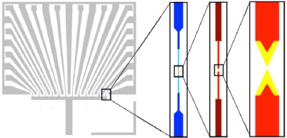
Figure 1. Schematic of the pattern layout of a 6 mm × 6 mm sample with eleven nanoelectrode pairs. Gray colored structures were created by optical lithography, while the colored structures were patterned by EBL (exposure dose of 350 µC cm−2 was applied for blue and 370 µC cm−2 for red and yellow structures; the relative exposure doses (REDs) were: 1.0 (dark blue), 1.1 (light blue), 1.0 (dark red), 1.2 (light red), 2.75 (yellow)).
Download figure:
Standard image2.2. Nanoelectrode fabrication
The fabrication of the nanostructure was performed in two steps. Firstly, the nanoelectrodes and connection pads were written by EBL (EBPG 5000+ from Vistec) in a 'lift-off' process. Secondly, 1–3 mm long and 30–150 µm wide connection lines, which overlap the previously created pads, and 250 × 250 µm2 contact pads were fabricated by optical lithography using a Karl Suss MA6 mask aligner in a second 'lift-off' process (figure 1, gray pattern). The connection of the nanoelectrode structures on the sample to the measurement equipment was performed by bonding wires.
2.3. Electron-beam lithography
In order to develop a reliable EBL fabrication process for nanoelectrodes with a separation of only a few nanometers the resist layer stack was optimized. Best results were obtained with a double layer resist stack of PMGI (1% polymethyl-glutarimide in cyclopentanone) and 25 nm PMMA (1% polymethyl-methacrylate in ethyl-lactate, molecular weight 950 K). PMGI (MicroChem) is especially optimized as an undercut layer in a double layer lift-off processing. The dissolution rate is optimized for undercut control and is influenced mainly by the pre-bake temperature. First, a 45 nm layer of PMGI was spin coated (0–4000RPM in 2 s, 4000RPM for 58 s), baked out for 7 min at 260 °C, and pre-exposed with UV-light (320 nm) in a mask aligner for 1 min. Next, a 25 nm layer of PMMA 950 K was spin coated (0–2000RPM in 5 s, 2000RPM for 55 s) and baked out for 7 min at 180 °C.
The nanoelectrode pattern design (shown in figure 1) was exposed using an electron beam with an acceleration voltage of 50 kV. The blue parts in figure 1 correspond to structures which were written with an exposure dose of 370 µC cm−2, a beam current of 5 nA and a beam step size of 20 nm (e-beam of 35 nm in diameter), while the red and yellow parts were written with the smallest stable e-beam with an exposure dose of 390 µC cm−2, a current of 60 pA and a beam step size of 1 nm. Additionally, the width of the nanoelectrodes was subsequently reduced from 10 µm/2 µm (dark blue), 1 µm (light blue), 200 nm (dark red) to 50 nm (light red). The reduced stray dose of the thinner nanoelectrodes was compensated by a higher relative exposure dose (RED) setting (coded by lighter colors in figure 1).
In order to fully exploit the possibilities of the double resist layer stack, we also worked out a two-step development process. After exposure, the PMMA was developed with isopropanol/water (7:3) for 80 s, a developer with high contrast and high sensitivity. Contrast curves for PMMA developed with various compositions of isopropanol/water and other developers are given in [15]. Additionally, the contrast curve for a PMMA layer processed according to our conditions is given in the supporting data (available at stacks.iop.org/Nano/23/125302/mmedia). The contrast value, γ, can be estimated to be 4.6 using the definition of the contrast of a positive tone resist: γ = 1/(log(D0/D1)), where D0 is the maximum dose at which still no resist is developed and D1 is the minimum dose at which all the resist is removed. The development of PMMA was stopped in demineralized water for 30 s and the sample was blown dry with nitrogen. Secondly the PMGI was developed with the metal-free alkaline developer MF21a (MicroChem) for 40 s, stopped in a demineralized water bath for 60 s, blown dry with nitrogen and baked for 2 min at 50 °C. The development rate of PMGI in this process was determined to be 4 nm s−1.
Subsequently, the deposition of a 1 nm Ti sticking layer and a 20 nm metal film was performed in an e-gun-evaporator under a pressure of <10−7 mbar. As electrode material Au, Pd or Pt can be chosen. In the lift-off process the double resist layer stack together with the covering metal was washed out with N-methyl-2-pyrrolidone for 2 h. Subsequently the chip was dipped in acetone for 2 min, rinsed with isopropanol and blown dry with nitrogen. After this process only the predefined nanoelectrode structures remain.
2.4. SEM
Scanning electron microscopy images of the nanoelectrodes were obtained with a Zeiss Gemini I, at 10 kV acceleration voltage.
2.5. Simulation
The scattering of a point sized electron beam in a realistic material stack (25 nm PMMA 950 K, 45 nm PMGI, 400 nm SiO2 on a bulk Si substrate) was calculated by a Monte Carlo simulation using the commercially available program 'Sceleton'. The realistic exposure dose profile was achieved by folding the result of the Monte Carlo simulation with a Gaussian electron beam.
3. Results and discussion
In EBL the resulting resolution is influenced by various factors, such as the e-beam pattern generator, the quality of the proximity correction, the resist-developer system, and the process parameter. Here, exposure is performed with a high resolution e-beam writer (Vistec) with high-energy electrons (between 50 and 100 keV acceleration voltage) and a spot size adjustable down to a few nanometer. A comparison of beam diameters obtained for acceleration voltages of 50 and 100 keV, respectively, is given in supporting data (available at stacks.iop.org/Nano/23/125302/mmedia). These measured diameters confirm the general rule that lower acceleration voltages lead to an increase in beam size and lower beam currents correspond to smaller beam sizes [13]. In order to achieve a small beam size and thus a high resolution we intentionally used the lowest stable beam current (60 pA) that was obtained for 50 keV.
The standard resist for high resolution EBL is PMMA that could be used to fabricate 5 nm wide lines at a pitch of 80 nm [13]. However, patterns collapse in dense structures, especially if thin resist layers are employed. On the other hand, even ultrathin resist layers are required to minimize the proximity effect in order to fabricate sub-5 nm structures. In a first approach to fabricate nanoelectrodes with a predefined separation of 5 nm we employed the double resist layer stack 40 nm PMMA–MAA and 20 nm PMMA which was processed as described in [12]. The mixed resist PMMA–MAA has a higher sensitivity than PMMA (see supporting data available at stacks.iop.org/Nano/23/125302/mmedia) and thus, in principle, is suitable as an undercut layer. However, one drawback of this double layer resist is that the development time depends on the necessary undercut for a reliable lift-off process. Hence it cannot be adjusted with regard to the stability of the mask bridge, i.e. the PMMA layer. A development time of 150 s was found to be the most suitable for the given conditions. The resulting nanoelectrode structures were characterized with SEM and the yield of usable electrode pairs with gap sizes between 5 and 9 nm was about 45%. The remaining nanoelectrode pairs were mostly shorted, pointing to a collapse of the mask bridge despite the fact that the structures were still underdeveloped (the size of the gap was larger than defined).
In a next step we applied the fabrication process described above, based on the double layer resist PMGI and PMMA, and thus were able to separate the development step for the mask layer (PMMA) from the development step necessary to create a suitable undercut. Hence, the above given development times are optimized in order to create a predefined nanoelectrode separation of 5 nm and a reliable lift-off process, respectively. The characterization of the resulting nanoelectrodes with SEM reveals that about 45% of the gap sizes are in the range of 4–6 nm, 10–20% of the gaps are larger and the remaining gaps are smaller than 4 nm but not necessarily shorted (figure 2). Thus, we were able to improve considerably the stability of the mask layer by using the improved resist-developer system. As a consequence a higher yield and a better structural control are achieved in the nanoelectrode fabrication process compared to standard resist layer stacks and developer.
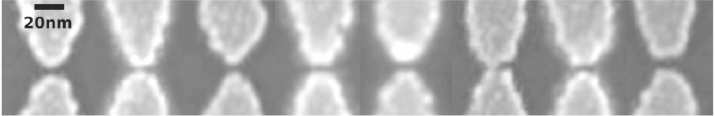
Figure 2. SEM images of nanoelectrode pairs of one sample: a tip separation of 4–6 nm within 45% was achieved (three short-circuited nanoelectrode pairs of the same run are not shown).
Download figure:
Standard image3.1. Short range proximity correction
Further attempts to reduce the nanoelectrode separation in the pattern design from 5 to 3 nm did not lead to better results. The remaining limit of the patterning accuracy could be attributed to proximity effects. Therefore we started to calculate the proximity effect related exposure dose.
Figure 3 shows the result of the simulation of a proximity effect corrected exposure dose profile performed with the program 'Sceleton' based on our material stack (25 nm PMMA, 45 nm PMGI, 400 nm SiO2, 100 µm Si). The black curve corresponds to the calculated relative exposure dose (CRED) as a function of the radial distance (r) from a point shaped electron beam. Additionally more realistic exposure dose profiles were achieved by folding this curve with a Gaussian beam with spot sizes of 2 nm, 3 nm and 4 nm in diameter, respectively (figure 3). The main difference between these effective dose profiles and the dose profile of an ideal, point-shaped electron beam is a considerably increased proximity effect related exposure dose, which is observed mainly in a radius of about 10 nm around the electron beam. Consequently, to avoid unintentional exposure in the gap between the nanoelectrodes, basically an electron beam with a very small diameter is required and the width of the electrode tips should be reduced in size. Already at a distance of 100 nm from the electron beam the relative dose is reduced to a millionth, so that the width of the electrodes at this distance from the electrode gap plays a minor role.
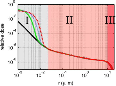
Figure 3. Proximity effect corrected exposure dose profile (CRED) calculated for a point-shaped electron beam as a function of the radial distance (r) (black curve). CREDs for a Gaussian beam with a spot size of 2 nm (green), 3 nm (blue) and 4 nm (red) are shown also. In the CRED profile three different sections (I–III) can be observed: (I) a Gaussian shape (gray background color), (II) an exponential decay (light red) and (III) a cut-off section (red).
Download figure:
Standard imageThe calculated exposure dose profiles, as shown in figure 3, exhibit three main sections: (I) a Gaussian shape in the central section for r < 20 nm, (II) an exponential decay in the intermediate section for 20 nm < r < 10 µm and (III) a cut off in the section for 10 µm < r < 20 µm. According to the dimension of section (I), the section of most intense exposure dose, the new electrode tips were designed as sharp spikes with three segments with a line width of 2 nm, 6 nm and 8 nm, respectively (figure 4). The length of the 50 nm and 200 nm wide electrode segments was extended to 2 µm and 18 µm, respectively, with regard to the dimensions of the sections (II) and (III) with the aim to ensure a good conductivity of the electrodes. Thus, an overall reduction of the area of the electrode structures of 77% compared to the original nanoelectrode design was performed in order to minimize backscattering.

Figure 4. In the new pattern design the length of the 200 and 50 nm wide lines (red) and the tip geometry were chosen according to the dimensions of the sections I–III of the CRED profile shown in figure 3 (background colors). Additionally the settings of the REDs were refined: 1.0 (dark blue), 1.1 (light blue), 1.0 (dark red), 1.3 (gray), 3.2 (brown), 6.0 (dark green).
Download figure:
Standard imageWith this optimized design, nanoelectrode pairs with separations of only 3 ± 1 nm were fabricated with a yield of 55%. Most of the inoperative nanoelectrode pairs were short-circuited. This points to the fact that the PMMA mask bridge is again a limiting factor for this ultrasmall pattern size. However, the fabrication of nanometer-scaled structures could be improved considerably by application of a new double resist layer stack, a high contrast developer and a pattern design based on the knowledge of an effective exposure dose profile. Thus, a structural control in the nanometer scale is achieved exemplified by the exact reproduction of the nanoelectrode design applying the fine-tuned EBL process (figure 5).

Figure 5. High resolution SEM of nanoelectrode pairs fabricated according to the first and the second electrode pattern design (compare figures 1 and 4). The electrode separation is reduced from 5 ± 1 n nm to 3 ± 1 nm, while the fabrication yield was improved to 55%.
Download figure:
Standard imageIn order to gain more insights into whether a contrast enhancement is achieved by the above-mentioned actions, we performed an analysis of the first and the second nanoelectrode pattern design (shown in figures 1 and 4, respectively). The realistic exposure dose was calculated pixel × pixel for both designs using the CRED profile of an electron beam. For this purpose the effective dose profiles for beam diameters of 2, 3 and 4 nm (see figure 3) were applied. Thus, we obtained CRED patterns for both nanoelectrode designs dependent on the electron-beam diameter (figure 6). In addition, the cross sections of the CRED patterns through the nanoelectrode gap position are shown in figure 7.
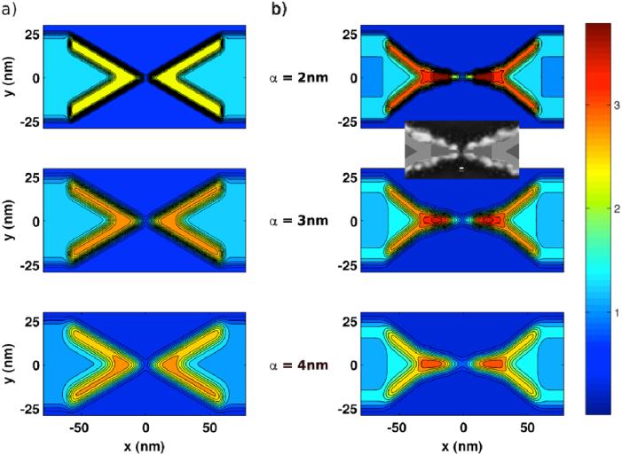
Figure 6. Simulation of the relative exposure dose pattern (CRED pattern) for beam diameters of 2 nm, 3 nm and 4 nm, respectively. The color coding describes the magnitude of the CRED. A good agreement between a scanning electron micrograph and the simulated dose pattern of a 2–3 nm beam was observed (see inset).
Download figure:
Standard image
Figure 7. Cross section through the gap position of the CRED pattern. The different beam diameters of 2 nm, 3 nm, 4 nm (green, blue, red) show a significant difference in contrast and dark exposure.
Download figure:
Standard imageA comparison of the cross sections of the CRED patterns reveals clearly that the contrast as well as the dark exposure are improved in the second nanoelectrode design. The higher contrast in the second effective dose pattern compared to the first dose pattern, that is the steeper crossover from the intentionally exposed to the unexposed resist between the nanoelectrode tips, can be deduced from figure 7 for each beam diameter under investigation. The higher contrast is due to the reduction of the exposed area and thus a reduced stray dose as well as to the high relative exposure dose of the electrode tips in the second design. Furthermore, the dark exposure in the center of the electrode tips was reduced from about CRED ∼0.54 in the first nanoelectrode design to CRED ∼0.35 in the second electrode design despite the increased RED settings of the electrode tips. Both effects together result in an control of electrode structures in the nanometer regime.
The SEM images of the fabricated nanoelectrodes are in good agreement with CRED patterns of the second electrode design for electron beams with spot sizes of 2 and 3 nm, see figures 5 and 6. Consequently the diameter of the used electron beam (60 pA at 50 keV) can be assumed to be 2.5 ± 1.0 nm. This spot size can be compared with the diameter of 3.9 nm deduced for an electron beam operated with a beam current of 140 pA at 100 keV acceleration voltage [16] within the limits of error.
The stability of the mask-bridge can be rated by the estimation of the remaining thickness after development. As described in [14] a relative dose of 0.35 of the necessary exposure dose corresponds to a remaining relative thickness of approximately 22 nm in the central part of the mask-bridge in the second nanoelectrode design. On the other hand, a relative dose of 0.80 of the necessary exposure dose corresponds to a remaining relative thickness of the resist layer of approximately 15 nm, which seems to be a stable thickness for the mask layer resist in boundary structures. A relative dose of 1.0 is reached for a nanoelectrode separation of 4 nm and ensures a safe development of the resist. This analysis again demonstrates the high contrast reached with this optimized fabrication procedure.
Besides the fabrication of nanoelectrode pairs with gaps down to 3 nm shown here, we also fabricated multi-electrode devices with electrode separations of a few nanometer. These results are given for interested readers in the supporting data (available at stacks.iop.org/Nano/23/125302/mmedia).
3.2. Current/voltage characteristics of lithographically defined nanoelectrode devices
Nanoelectrodes with separations of ∼2 nm are known to show tunneling characteristics which can be interpreted within the Simmons model [17–19]. In order to perform test measurements the lithographically fabricated nanoelectrodes using the second pattern design were bonded to a chip carrier and connected to a measurement equipment especially suited for low current measurements. One out of ten nanoelectrode pairs exhibited a tunneling characteristic with an exponential behavior (shown in figure 8) which can be described within the Simmons model [17]. An iterative fitting sequence, as published previously [18], revealed a height of the tunneling barrier of Φ = 4.9 ± 0.1 eV and a nanoelectrode separation of 2.2 ± 0.1 nm. This measurement demonstrated that nanoelectrodes useful for transport investigations on nanoscale building blocks have been fabricated by an optimized EBL procedure.
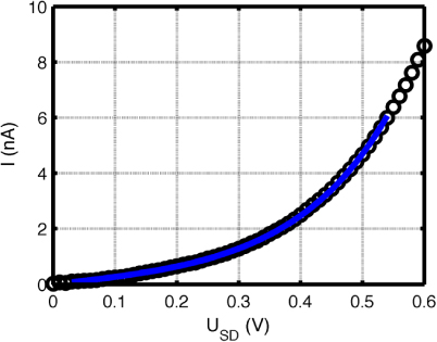
Figure 8. Tunneling characteristic measured between nanoelectrodes with a separation of <3 nm. The blue line represents a Simmons fit according to a routine described in [18]. Thus, a barrier height of Φ = (4.9 ± 0.1) eV and an electrode separation d = (2.2 ± 0.1) nm were obtained, corresponding to a vacuum gap between metallic electrodes.
Download figure:
Standard image4. Conclusion
The EBL process was improved by the use of an optimized double layer resist stack (PMGI and PMMA) and by an attuned two-step development process. In consequence it was possible to steer the undercut of the resist profile and thus the stability of the mask bridge. These improvements resulted in nanoelectrode pairs with a separation of 4–6 nm.
However, the realistic simulation of the proximity effect related exposure dose and the development of a new nanoelectrode design based on the knowledge of these data resulted in a structural control of the nanoelectrodes defined by the EBL process and nanoelectrode separations of 3 ± 1 nm.
Acknowledgments
The authors gratefully acknowledge the help of N Babajani, M Grates, R Borowski and H Haselier. This work was partially supported by the EU FP7 project 'MOLOC' and the 'Deutsche Forschungsgemeinschaft' (DFG).