

Abstract
The ability to selectively chemically functionalize silicon nitride (Si3N4) or silicon dioxide (SiO2) surfaces after cleaning would open interesting technological applications. In order to achieve this goal, the chemical composition of surfaces needs to be carefully characterized so that target chemical reactions can proceed on only one surface at a time. While wet-chemically cleaned silicon dioxide surfaces have been shown to be terminated with surficial Si–OH sites, chemical composition of the HF-etched silicon nitride surfaces is more controversial. In this work, we removed the native oxide under various aqueous HF-etching conditions and studied the chemical nature of the resulting Si3N4 surfaces using infrared absorption spectroscopy (IRAS), x-ray photoelectron spectroscopy (XPS), low energy ion scattering (LEIS), and contact angle measurements. We find that HF-etched silicon nitride surfaces are terminated by surficial Si–F and Si–OH bonds, with slightly subsurface Si–OH, Si–O–Si, and Si–NH2 groups. The concentration of surficial Si–F sites is not dependent on HF concentration, but the distribution of oxygen and Si–NH2 displays a weak dependence. The Si–OH groups of the etched nitride surface are shown to react in a similar manner to the Si–OH sites on SiO2, and therefore no selectivity was found. Chemical selectivity was, however, demonstrated by first reacting the –NH2 groups on the etched nitride surface with aldehyde molecules, which do not react with the Si–OH sites on a SiO2 surface, and then using trichloro-organosilanes for selective reaction only on the SiO2 surface (no reactivity on the aldehyde-terminated Si3N4 surface).
Export citation and abstract BibTeX RIS
1. Introduction
Silicon nitride (SixNy) and silicon oxide (SiOx) are important materials within integrated devices of multiple applications from the microelectronics industry to the sensing and electro-mechanical communities (NEMS/MEMS). In many applications, the surfaces of both of these materials (and perhaps many others materials as well) will be treated concurrently during chemical processing. For many device applications in the microelectronics industry, there is a desire to chemically functionalize only one of the exposed materials present on an integrated structure, which may contain many exposed materials such as silicon nitride, silicon oxide, carbon hardmask, amorphous silicon, metal oxide, metal nitride, and/or metallic interconnects, barriers, and liners. Each surface must be chemically terminated with unique functional groups that allow for the growth of a distinct material on its surface. Clearly, the requirements for chemical specificity become more challenging depending on the number of unique materials exposed during processing.
To address a system of interest to microelectronics industry and show a proof-of-concept, this work focuses on only two materials, schematically represented by C and D in scheme 1, which need to be differently functionalized to deposit 2 different materials, A and B. Here, material C is silicon nitride (Si3N4), and material D is silicon dioxide (SiO2). For a proof-of-concept experiment on these thin film materials, material A is an organic aldehyde arranged as a self-assembled monolayer (SAM), and material B is a different SAM generated from chlorosilane or ethoxysilane molecules.

Scheme 1. Schematic cross-sectional side view (left) for a generic integrated structure involving two materials C, and D, and substrate F. Under some integration schemes, it would be desired to have new material, A, deposited only on top of material C and not on material D (middle). Later in the integration, it might be desired to have a new material, B, deposited only on top of material D and not on material A; material C is assumed to be completely covered by A and therefore not available for reaction during deposition of material B (right).
Download figure:
Standard image High-resolution imageA first step toward achieving selectivity of deposition is to understand the chemical termination of the silicon dioxide and silicon nitride materials. Many reports have shown that wet-chemically processed silicon dioxide is terminated by atop Si–OH groups [1–4], which can react with alkoxy- and/or chloro-organosilanes [1, 4–7]. While the preparation and growth of clean Si3N4 surfaces has been examined [8–14], the subsequent processing and surface chemistry remains quite controversial. Upon air exposure, silicon nitride materials grow a silicon-rich and nitrogen-depleted native oxide [15–17], which is expected to be terminated by Si–OH sites similar to those present on the silicon dioxide surface. Even if the bulk compositions of these two materials are different, similar surface chemical species are expected to significantly reduce the selectivity in the deposition of new materials. To this end, removal of the native oxide on the silicon nitride is expected to be a critical step in producing unique surface chemical species. Various cleaning and etching processes have been explored both experimentally and theoretically [17–23]. It has been shown that aqueous fluoride solutions are able to remove the native oxide on Si3N4, but the reported surface chemical termination after etching varied from −NHx [24], Si–H [25], to fluorine [26]. Consistent with some of these assignments, compelling evidence for their reaction includes the reaction of Si–H bonds to form of Si–C bonds using the hydrosilylation techniques [27] and reaction of NHx groups with aldehydes via a Schiff base [28] reaction. The lack of consistency among the different reports may stem from a variations in chemical preparation or variations in the bulk material either in terms of their density and/or internal concentrations of Si–H and NHx sites, which can strongly depend on the deposition conditions.
The main goals of this work are to fully characterize the nominally stoichiometric Si3N4 grown by chemical vapor deposition (CVD), its changes upon HF etching, and its suitability for selective deposition reactions in the presence of silicon dioxide. Recently, we reported on a preliminary characterization of this material indicating the need for a deionized water (DI) rinse to achieve a smooth partially fluorine-terminated surface void of etching byproduct salts that can significantly complicate chemical analysis [29]. Herein, we significantly build upon this work by combining x-ray photoelectron spectroscopy (XPS), low-energy ion scattering (LEIS), gas cluster ion beam treatment (GCIB), and infrared absorption spectroscopy (IRAS) to quantify the thermal stability, reactivity, and coverage of the atop Si–F, Si–O, and Si–NH2 chemical functionalities. Then, we use this knowledge to propose and test a processing sequence that leads to selective functionalization.
2. Experimental section
2.1. Materials
The following chemicals were used as received without further purification: anhydrous toluene (Sigma), anhydrous methanol (Sigma), dichloromethane (Fisher Scientific), acetone (Fisher), 30% hydrogen peroxide (H2O2, Fisher), and ammonium hydroxide (NH4OH, Certified ACS Plus, Fisher). The following organosilane molecules were purchased from Gelest Corporation and used as received: octadecyltrichlorosilane (ODTCS, CH3(CH2)17SiCl3), n-octadecyltriethoxysilane (ODTES, CH3(CH2)17Si(OC2H5)3), chlorodimethyloctadecylsilane (CDMODS, CH3(CH2)17Si(CH3)2Cl), and 11-aminoundecyltriethoxysilane (AUTES, NH2(CH2)11Si(OC2H5)3). Undecanal (UDA) (97%) was obtained from Aldrich and used as received. Purified deionized water (DI) was provided by a Millipore filtration system with a nominal resistivity of 18.5 MΩ cm. Hydrofluoric acid (J.T. Baker, 49%) was diluted with DI to concentrations of 0.1% (0.03 M), 1% (0.32 M), or 10% (3.18 M).
2.2. Surface cleaning and etching
Intel Corporation provided 30 nm thick nominally stoichiometric Si3N4 films grown on both sides of double-side polished native oxide terminated B-doped CZ p-Si(1 0 0) wafers. A similar technique was used to grow 30 nm of SiO2 on both sides of other wafers. Both surfaces were probed by transmission IR spectroscopy and were active for chemical reaction and analysis. Wafers were cut into 1.5 inch × 0.6 inch (3.8 cm ×1.5 cm) rectangular pieces, degreased by sequential sonication in dichloromethane, acetone and methanol for 10 min each, rinsed under flowing DI, and dried under a flowing stream of nitrogen gas, N2(g). The degreased Si3N4 samples or coupons were then put in the FTIR spectrometer to record a background/reference spectrum. Coupons were then etched for various times from 1–6 min in different concentrations of HF(aq) from 0.1% to 49%, immediately rinsed with flowing DI for 30 s, dried with N2(g) and examined by IR spectroscopy or other techniques within minutes. An important factor to obtain clean surfaces (i.e. without remnant etching products) is to ensure that the sample stays wet (i.e. never dries) as it moves from the HF(aq) etching solution to the water rinsing step.
2.3. Alkylsiloxane reaction conditions
Glass reaction tubes were pre-treated with reaction chemicals at 70 °C for 1 h in order to make the inner glass surface hydrophobic and clean. The chemicals were then discarded from the reaction tubes and replaced with 20 ml of fresh 1 mM toluene solutions of ODTCS, ODTES, CDMODS, or AUTES. Freshly etched, rinsed, and dried Si3N4 or SiO2 coupons were placed each into a separate glass reaction tube and allowed to react at 70 °C for 1 h. Upon completion, the coupon was removed from the tube, quickly rinsed with toluene, and dried. All surface modification reactions were performed under a nitrogen atmosphere.
2.4. SC-1 treatment on alkylsiloxane-terminated surfaces
The stability of alkylsiloxane-modified surfaces of Si3N4 or SiO2 was tested by a 10 min immersion in a 80 °C SC-1 solution (5 : 1 : 1 volume ratio of H2O: 30% H2O2(aq) : concentrated NH4OH). Upon completion, the coupons were rinsed extensively with DI and dried under N2(g). All surface treatments and surface rinsing were performed under ambient condition.
2.5. Aldehyde reaction conditions
Freshly HF-etched, rinsed, and dried Si3N4 and SiO2 coupons were placed separately into rinsed screw-capped vials containing a solution of 0.4 M undecanal in methanol. The reaction was carried out at 65 °C under nitrogen atmosphere for 16 h. Upon completion, coupons were removed from the vial, immediately rinsed with fresh methanol, sonicated for 5 min in dichloromethane, and dried under a stream of nitrogen. Coupons were stored in a glovebox between measurements and rinsed with fresh dichloromethane and dried under argon prior to characterization.
2.6. Surface characterization techniques: IRAS, XPS, GCIB, LEIS, contact angle, and AFM
Infrared absorption spectroscopy (IRAS) was performed with a N2-purged Fourier transform infrared spectrometer (FTIR) in transmission mode at an angle of incidence of 74° with respect to the Si surface normal (Brewster angle for Si) using a pyroelectric DTGS detector. Five loops of 1000 scans each were obtained prior to and after each particular chemical step of interest, then averaged as needed to minimize noise without deteriorating the base line. The final absorption spectrum was obtained from the averaged sample and reference spectra.
XPS were obtained with a PHI Versa Probe II scanning XPS microprobe, Physical Electronics, United States spectrometer, equipped with a concentric hemispherical analyzer under ultrahigh vacuum conditions (4.8 × 10⁻⁸ Pa), using an Al Kα monochromated x-ray source. Surfaces were analyzed with a 45° takeoff angle; a 187 eV pass energy was used for survey spectra and a 11.75 eV pass energy for high resolution scans. The XPS chamber was equipped with two kinds of sputter guns: (1) an Ar+ sputter gun generating a beam of Ar ions with an energy variable from 250 eV to 5 kV, and (2) a gas cluster ion beam (CGIB) to produce Ar clusters ranging from 1000 to 2500 atoms/cluster with kinetic energies ranging from 5 to 25 kV. During sputtering, the pressure in the chamber was maintained at 2 × 10⁻⁶ Pa. A raster size of 1 mm ×1 mm was chosen for the Ar GCIB sputtering process to ensure a larger area was processed relative to the 100 μm diameter region probed during XPS analysis. The XPS spectra were analyzed using the CASA XPS software using sensitivity factors taken from the MultiPak version 6.0 software (supplied by Physical Electronics). Due to the surface charging of insulating silicon nitride thin films, XPS core level spectra peak values typically shifted to a +1.3 eV high binding energy, typically corrected by fixing the C 1s peak (from adsorbed hydrocarbons) at 284.5 eV.
LEIS analysis was performed in a chamber equipped with an IonTOF Qtac100 detector using 3 keV 4He+ under UHV conditions (base pressure <7 × 10⁻¹⁰ mbar). Typical measurements used a target ion current in the range of 2–4 nA. The ion beam was focused on a 1 mm × 1 mm sample area at normal incidence. The technique is intrinsically surface sensitive (~3 monolayers) due to a strong interaction between low energy ions and surface atoms. The overall sensitivity originates from a unique analyzer detector design, where a large scatter angle of detection (fixed scattering angle = 145°) increases the count rate, allowing use of low ion doses (negligible sputtering/intermixing) [30]. Each element in the LEIS spectra was quantified by fitting an error function and Gaussian curve to the element in question and using the area of the Gaussian curve as the integrated area. The detection of carbon and nitrogen is complicated by two phenomena, however. The energy of backscattered 4He+ from carbon near 850 eV that would be detected by LEIS covers a broad range of the low energy spectrum (⩽700 eV) due to re-ionized He atoms and sputtered H atoms, which makes the detection of surface carbon difficult. Further, LEIS has a low sensitivity to nitrogen due to the high neutralization probability of the 4He+ when interacting with nitrogen [30]. Since LEIS mostly probes the surface, surface contaminants are often a problem, requiring precleaning before data are taken. In our case, great care was taken to rapidly transfer (<5 min) freshly etched or chemically processed samples into the LEIS vacuum chamber and to perform a mild anneal (80–90 °C for 5 min) once in ultra-high vacuum to desorb possible physisorbed species.
For the IR, XPS and LEIS measurements, the samples are held by Ta clips and heated resistively. The temperature is monitored by a Chromel–Alumel thermocouple welded to a Ta clip that is attached in the middle of the long edge of the sample (i.e. equidistant from the clips).
Static water contact angle measurements using a 2 μl drop size were performed on a standard goniometer from Ramé-hart instruments, Co (model 200-F), with a typical error of ±1°. Atomic force microscopy (AFM) images were recorded with a Veeco Digital Instrument Nanoscope Dimension 3100 in ambient atmosphere. All the measurements were performed in tapping mode with a resolution of 512 points per line.
3. Results and discussions
This section comprises three distinct parts. The first part (section 3.1) addresses the chemical composition and stability of HF(aq)-etched, water rinsed, and dried Si3N4 films, including subsequent stability in aqueous environments. The second part (section 3.2) uses this knowledge to investigate grafting of a variety of molecules, in particular silanes and aldehydes, on the HF(aq)-etched, water rinsed and dried Si3N4 or SiO2 surfaces. The results demonstrate that selective chemical functionalization can be achieved. The last section (section 3.3) proposes mechanisms to account for the observed surface termination after HF(aq) etching, water rinsing, and drying.
3.1. Chemical composition and stability of HF-etched Si3N4 films
We have previously shown that the surface chemical composition of CVD-grown Si3N4 thin films after aqueous HF etching and water rinsing is dominated by a significant amount of fluorine, oxygen, and carbon, but no evidence for Si–H bonds is observed even after significant water rinsing [29]. The post-etch water rinsing step was shown to be critical to remove etch byproduct salts such as (NH4)2SiF6 from the surface, thus ensuring surface cleanliness. Because these results are in apparent contradiction to some of the published work [24–26, 28], we need to examine the role of parameters such as HF concentration and silicon nitride composition (i.e. bulk Si–H and NHx concentration) on the resulting surface chemical composition.
In order to accomplish this, we first examine the surface fluorine and oxygen content as a function of HF concentration (0.1, 1, and 10%) by XPS and LEIS (section 3.1.1). Further chemical bonding information of the surface fluorine and oxygen species is extracted from gas cluster ion beams (GCIB) in conjunction with XPS analysis and from LEIS measurements as function of temperature (section 3.1.2); the fluorine coverage is then quantified in section 3.1.3. Evidence for amine termination (N–Hx) is derived from detailed IRAS measurements after HF etching in 1%, 10%, and 49% HF solutions (section 3.1.4). However, quantification of surface OH and NHx coverages can only be performed by wet chemical titration, and will be addressed later in section 3.2 that deals with wet chemical surface functionalization. Therefore, in preparation for section 3.2, the stability of the HF-etched Si3N4 surface in water, which is a typical trace contaminant during wet chemical reactions, is examined in section 3.1.5.
3.1.1. Characterization of HF-etched Si3N4 samples.
The elemental surface composition is studied by XPS and LEIS only on surfaces that have been solvent-degreased and etched in HF(aq) (0.1%, 1%, and 10%) for 4 min followed by an immediate rinse with deionized water and then dried in N2, as shown in figures 1 and S1 (stacks.iop.org/JPhysCM/28/094014/mmedia). The high resolution F 1s core level spectra are shown in figure 1(A) and the analysis of the signal after normalization of the signal relative to the silicon peak is summarized in table 1 as a function of HF concentration (0.1%–10%). Note that all F 1s peaks shown in figure 1(A) are symmetrical, with similar FWHM, and are therefore consistent with a single species. Note that there is no detectable component of the N 1s core level between 403–405 eV (see figure S1) (stacks.iop.org/JPhysCM/28/094014/mmedia), indicating that there are no N–F bonds [31]. LEIS spectra of degreased Si3N4 samples after a 1 min etch in 10% HF(aq) (figure 1(B), red line) and 1% HF(aq) (figure 1(B), blue line) show similar F (1310 eV) quantities, as summarized in table 1, even though there is a measurable difference in the O (1122 eV) and Si (1670 eV) integrated areas for 1% HF and 10% HF etch treatment.
Table 1. Summary of XPS and LEIS data parameters for Si3N4 etched with either 0.1%, 1%, or 10% HF(aq).
| HF concentration (M) | XPS data | LEIS data | |||||
|---|---|---|---|---|---|---|---|
| F 1s peak position (eV) | F 1s peak area | FWHM | F/Si area ratio | F peak area | O peak area | Si peak area | |
| 0.03 (0.1%) | 688.3 ± 0.1 | 870 ± 78 | 1.58 ± 0.09 | 0.21 ± 0.04 | — | — | — |
| 0.32 (1%) | 688.3 ± 0.1 | 961 ± 36 | 1.58 ± 0.06 | 0.24 ± 0.03 | 252 ± 10 | 81 ± 8 | 164 ± 9 |
| 3.18 (10%) | 688.2 ± 0.2 | 1021 ± 74 | 1.72 ± 0.07 | 0.25 ± 0.02 | 267 ± 11 | 42 ± 7 | 233 ± 10 |
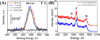
Figure 1. (A) X-ray photoelectron spectra of the F 1s core level of degreased Si3N4 reference surface (black line) and after a 4 min etch by either 10% (red line), 1% (blue line), or 0.1% (green line) HF(aq), rinsed immediately with DI, and dried under N2(g); (B) LEIS measurements of degreased Si3N4 surfaces after a 1 min etch in 10% HF(aq) (red line) or in 1% HF(aq) (blue line), rinsed immediately with DI, and dried under N2(g); LEIS measurements were not performed for 0.1% HF since XPS data did not show any significant difference. No surface sputtering was performed for any samples.
Download figure:
Standard image High-resolution imageAll these data indicate that the originally F-free surface is covered by similar amount of F after HF(aq) etching, independent of HF concentration, even though different amounts of Si3N4 are removed by etching. The F 1s peak is centered at 688.3 ± 0.1 eV (688.2 ± 0.2 eV for 10% HF), which is consistent with the presence of a Si–F bond [32, 33]. Since LEIS is much more surface sensitive than XPS, these results confirm that Si–F is at the surface. The discrepancy in O and Si quantities observed in LEIS can be explained by the work of Bermudez [18, 19], who showed that etching in dilute 0.01–0.02 M HF(aq) can result in a significant amount of oxygen at the surface. While the HF(aq) concentration may lead to some change in the amount of surficial oxygen in our data, tentatively assigned to Si–OH groups, it comes as a reduction in the amount of detectable Si with no significant change in the surficial F content. There is also no strong signal assigned to nitrogen in LEIS, due to a high neutralization probability of the helium ions when interacting with nitrogen [30]. While there might be some available Si–NHx species near the surface of the film, there are expected to be either too low in concentration and/or sufficiently subsurface to be detected by LEIS.
3.1.2. Chemical bonding of fluorine and oxygen on HF-etched Si3N4 surfaces.
Since our previous work showed that salt byproducts could easily be adsorbed [29], we used gas cluster ion beams (GCIB) of various intensities and times to distinguish between covalently bound F (e.g. Si–F) and potentially physisorbed F-containing salts. After etching a Si3N4 sample for 4 min in 1% HF(aq) and rinsing in water for 30 s, the resulting high resolution XPS spectra show the presence of fluorine (figure 2(A) (a), black line) and carbon (figure 2(B) (a), black line). Upon exposure of the HF(aq) etched Si3N4 surface to the most gentle sputtering condition, a 5 kV 2500-atom cluster (i.e. 2 eV per Ar atom), the C is nearly completely removed (figure 2(B) (b), red line) while the F is only reduced to 87 ± 14% of its initial amount (figure 2(A) (b), red line). Note that the F 1s peak does not significantly change in area when exposed to this gas cluster condition a second time (figure 2(A) (c), pink line). These observations are consistent with the carbon being physisorbed (e.g. adventitious), but the majority of fluorine being chemically bound.

Figure 2. Comparison of XPS (A) F 1s, (B) C 1s, and (C) O 1s spectra of a Si3N4 surface after a 4 min 1% HF(aq) etch, 30 s DI water rinse, and N2(g) dry (a), and after various GCIB treatments: 5 kVMax2500 1 × 1 GCIB sputtering for total times of 0.5 min (b) for 1 min (c), and then after 10 kVMax2500 1 × 1 GCIB sputtering for total times of 0.25 min (d), 0.75 min (e), 2 min (f), 6 min (g), 11 min (h), and 16 min (i), respectively. Insets show the corresponding F 1s, C 1s, and O 1s core level spectra overlaid.
Download figure:
Standard image High-resolution imageUpon exposure of the sample to Ar cluster beam of higher energy (e.g. a 10 kV 2000-atom cluster, i.e. 5 eV per Ar atom), the integrated areas of the F 1s peak slowly drop to zero over a range of exposure times between 0.25 to 16 min (figure 2(A) (d)–(i), orange line to purple line). The sputtering results indicate that chemisorbed F atoms (e.g. atop Si–F bonds) are located at the very surface, i.e. not positioned subsurface as observed after plasma treatment [34].
Oxygen 1s XPS core level spectra were measured at the same time as the F 1s and C 1s spectra of figures 2(A) and (B), and the results are displayed in figure 2(C) using the same color coding for the GCIB treatment conditions as in figures 2(A) and (B). There are 2 key observations: first, the O 1s peaks do not decay as quickly as the F 1s peaks in figure 2(A); and second, the O 1s spectra show a significant shift (1.6 eV) in peak binding energy from 534.4 to 532.8 eV as the sputtering time is increased. While the position of the F 1s peak in figure 2(A) also shifts by about 1 eV over the course of the GCIB sputtering, the shift in the O 1s spectra is nearly twice as large; the core level shift for O 1s therefore cannot be explained entirely by sample charging but likely represents a transition in the chemical state of oxygen as the GCIB sputters into the subsurface.
The first observation implies that the presence of oxygen either persists deeper into the bulk of the film than fluorine or is more tightly bonded at the surface and therefore not as easily removed. The second observation indicated that different oxygen environments exist at the surface and below the surface. From these results, we propose that the etched Si3N4 surface contains both atop Si–OH and Si–F sites and that the immediate subsurface contains some back-bonded Si–O–Si (or possibly buried Si–OH) moieties. Note that as the atop Si–F and Si–OH sites are removed through GCIB sputtering, the relative XPS integrated area for O in backbonded Si–O–Si and/or buried Si–OH will increase slightly due to the absence of screening from the atop layer. The estimates of F and surface OH coverages will be presented in sections 3.1.3 and 3.2.1.
An additional check of the chemical bonding of surface fluorine can be obtained by measuring the thermal stability of a HF(aq)-etched Si3N4 surface from 30–950 °C using in situ UHV annealing within the LEIS chamber. The results are shown in figure 3(a) for a degreased Si3N4 surface etched for 1 min in 1% HF(aq) etch, immediately rinsed in DI, dried under N2(g), and loaded into the LEIS chamber. LEIS measurements are performed at 30 °C at several spots on the surface between each subsequent 1 min-anneal at 100, 200, 300, 400, 500, 600, 700, 800, and 950 °C.
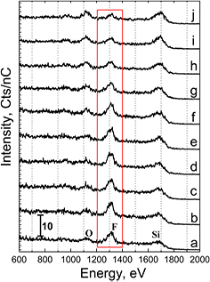
Figure 3. LEIS spectra after different thermal treatments: (a) a degreased Si3N4 surface after a 1 min 1% HF(aq) etch, immediate DI rinse, and N2(g) dry measured at 30 °C followed by a sequence of in situ UHV 1 min anneals at (b) 100 °C, (c) 200 °C, (d) 300 °C, (e) 400 °C, (f) 500 °C, (g) 600 °C, (h) 700 °C, (i) 800 °C, and (j) 950 °C respectively. No sputtering of the surface was performed prior to analysis.
Download figure:
Standard image High-resolution imageThe initial post-etch spectrum, measured at 30 °C without any sputtering (figure 3(a)), is consistent with that shown in figure 1(B). The integrated area of each element are measured and summarized in figure 4. Between 30 and 200 °C, 92 ± 3% of the starting F peak area is retained. This implies that only a small amount of the total F is easily removed (traces of physisorbed salts), which is consistent with the small loss of some F species under the least aggressive GCIB sputter of figure 2(A) (b). From 200 °C to 500 °C, the fluorine integrated area remains remarkably unchanged, as would be expected for the strong bond energy of the Si–F species (540 kJ mol−1). Above 500 °C, the F integrated area decays, and due to reduced screening by its absence, the intensities of Si and O fractionally increase. As LEIS is sensitive to only the top 1–2 monolayers of atoms on a surface [30], the fractional increase in O as F thermally desorbs is consistent with the conclusion (figure 2) that some oxygen exists as backbonded subsurface Si–O–Si and/or subsurface Si–OH species, not just as surficial Si–OH sites.
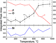
Figure 4. LEIS integrated peak areas of Si, F, and O versus temperature. There is a clear trend of decrease in F, increase in O, and a slight increase in Si upon increasing annealing temperature. Error bars represent the error in peak area obtained by fitting using different baseline positions.
Download figure:
Standard image High-resolution image3.1.3. Quantification of fluorine surface coverage on HF-etched Si3N4.
The fluorine coverage was found to be independent of HF concentration. Therefore, for quantification purposes, we measured the XPS F 1s peak areas from Si3N4 surfaces etched in 10% HF(aq) for 1 min, DI rinsed, and N2(g) dried, and compared them to silicon surfaces prepared to produce exactly 1/3 monolayer (ML) fluorine [35, 36] (figure 5). Assuming that the F atoms on the flat Si(1 1 1) surfaces and etched nitride surface have the same sensitivity factor, we find that the coverage of the HF-etched Si3N4 films is 0.70 ± 0.02 ML, regardless of the HF(aq) concentration (figure 1(A)), based on the integrated area ratio (see section S1 in supplementary information for consideration of this estimate) (stacks.iop.org/JPhysCM/28/094014/mmedia). The shift in the position of the F 1s peak is due to the difference in electronic environment between the HF(aq)-etched, DI rinsed, and N2(g) dried Si3N4 surface, where the Si–F sites contain backbonds to more electronegative N (or O) atoms relative to the 1/3 F-Si(1 1 1) surface sites which contain backbonds to less electronegative Si atoms of the single crystal wafer.
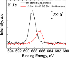
Figure 5. XPS F 1s core level of a Si(1 1 1) surface with 0.33 ML F (red line) and a HF-etched Si3N4 surface (black line). Comparison of integrated areas results in a surface F coverage of 0.70 ± 0.02 ML for the silicon nitride sample etched in 10% HF for 1 min, immediately rinsed in DI, and N2(g) dried.
Download figure:
Standard image High-resolution image3.1.4. Detection of surficial Si–NH2 bonds on HF-etched Si3N4 surfaces.
In addition to fluorine and oxygen, amine termination has also been reported. We have therefore examined the IR spectra of HF-etched, DI rinsed, and N2(g) dried surfaces very carefully, as no strong absorption related to N–H bonds was initially easily observed because there are some NH2 species in the nitride film itself. In order to distinguish surface and bulk species observed on the IRAS spectra, a longer etch (6 min) was performed relative to the typical 1 min etch using different HF(aq) concentrations of 1%, 10%, and 49% on nominally identical coupons (figure 6). The last concentration (49%) is purposefully used to completely remove the Si3N4 film and to expose the Si substrate, thus providing quantitative information for species contained in the Si3N4 film. All spectra are referenced to the degreased Si3N4 film prior to HF etching, immediate DI rinsing, and N2(g) drying.
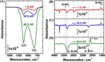
Figure 6. Differential infrared absorption spectra: (A) lower frequency region, and (B),(C),(D) higher frequency region showing the degreased Si3N4 surfaces after 6 min etch with either 1% HF(aq) (red line), 10% HF(aq) (blue line), or 49% HF(aq) (green line), followed by immediate DI rinse and N2(g) dry. All spectra are referenced to the degreased Si3N4 surface prior to HF etching.
Download figure:
Standard image High-resolution imageAfter 6 min etching in 1% HF(aq) concentration, immediate DI rinsing, and N2(g) drying the IRAS spectrum is consistent with the Si3N4 etching results from LEIS and XPS reported above but with more bulk Si3N4 material removed due to the longer etch time. In addition to the typical negative absorption bands observed for the Si3N4 TO and LO phonons modes at 838 and 1122 cm−1 (figure 6(A)), two other negative modes (figures 6(B)–(D)) at 2207 cm−1 (buried bulk species of Si–H) and 3342 cm−1 (buried bulk species of Si–NH2) are observed. Such buried species are typical of CVD-based processes, which generate relatively small amounts of NHx defects in the Si3N4 bulk material during deposition [37] that can only be observed once sufficient nitride is etched away.
The key observation is the appearance of two very weak, but positive, bands (~1 × 10⁻⁴ absorbance) at 1550 and at 3426 cm−1, which are assigned to the Si–NH2 deformation and the N–H stretch of the Si–NH2 species, respectively [38]. These frequencies are different from those of byproduct salts seen on improperly rinsed Si3N4 surfaces after an HF(aq) etch [29], and are therefore attributed to NH2 species at the surface. This is confirmed by increasing the HF concentration. While there is notably more removal of Si3N4 film (i.e. larger loss of bulk Si–H, Si–NH2, and the Si3N4 LO and TO phonon modes), the integrated areas of the 1550 cm−1 Si–NH2 modes remains similar (peak area of 1% HF(aq) etch case: 0.004 31 ± 0.000 10 cm−1; peak area of 10% HF(aq) etch case: 0.005 75 ± 0.000 15 cm−1), consistent with a chemisorbed surface species. If we turn to the oxygen concentration at the surface as determined from LEIS data (figure 1 and table 1), we note that there is a higher O content for the 1% HF(aq) etched surface than for the 10% HF(aq) etched surface. This observation, together with the fact that the F coverage remains the same for all HF(aq) concentrations, suggests that the remaining sites on the surface (i.e. sites that are not F terminated) are divided among oxygen (Si–OH and/or Si–O–Si) and Si–NH2, where surfaces etched with the lower concentration of HF(aq) experimentally have more O and less Si–NH2 than surfaces etched with a higher HF concentration.
As mentioned above, etching the Si3N4 film with 49% HF(aq) for 6 min results in complete removal of the 30 nm Si3N4 film as well as the underlying native silicon oxide on the Si(1 0 0) surface, leading to H termination of the exposed Si(1 0 0) surface. Figure 6(D) shows the appearance of strong positive Si–H modes at 2107 cm−1 that are typically found on the oxide-free HF-etched Si(1 0 0) surfaces. Concurrently, once the 30 nm Si3N4 layer is completely removed, the 1550 cm−1 mode assigned to the Si–NH2 also disappears since the H–Si(1 0 0) surface does not contain this surface species; this result provides additional confirmation of its assignment. The quantification of the NH2 coverage will be given in section 3.2.4 because it will require aldehyde functionalization (see section S1 in supplementary information for consideration of these estimates) (stacks.iop.org/JPhysCM/28/094014/mmedia).
3.1.5. Stability of the HF(aq)-etched Si3N4 surface in water.
Since wet chemical functionalization is essential for quantifying OH and NH2 surface concentrations and since water rinsing is part of the cleaning process, it is important to investigate the stability of these HF(aq)-etched silicon nitride films in water. While the Si–F bond is strong, we have previously shown that it can be transformed into Si–OH by immersion in pure water for several minutes on a Si(1 1 1) substrate [36]. However, the reactivity of HF(aq)-etched Si3N4 surfaces may be quite different from that of Si–F on Si(1 1 1). We have therefore investigated its stability in both cold and hot water. For these experiments, degreased Si3N4 samples were etched in 10% HF(aq) for 4 min, rinsed immediately in DI, dried under N2(g), measured in XPS and/or LEIS, and then immersed in, or rinsed under, DI at 23 °C or 70 °C for various immersion times. Figure 7(A) shows the F 1s high resolution region after HF(aq) etch, DI rinse, and N2(g) dry, and subsequent immersion in 23 °C DI for 1 min, and then 1, 4, 24, and 48 h. Most of the fluorine is removed within 24 h in 23 °C water. Similar fluorine removal kinetics (figure 7(B)) is observed when the sample is actively rinsed under flowing DI water at room temperature. When immersed in 70 °C DI, however, the removal of fluorine is much more rapid, with only 28 % ± 4% of the starting fluorine area remaining after 30 min (figure 7(C)). For this 70 °C DI immersion experiment, the XPS O 1s peak area increases by 224% ± 45% after 30 min of immersion time (figure 7(D)). As the XPS probes 5–10 nm of the near surface region, the increase in oxygen could come from an increase in the surficial O concentration, an increase in subsurface oxidation, or both.
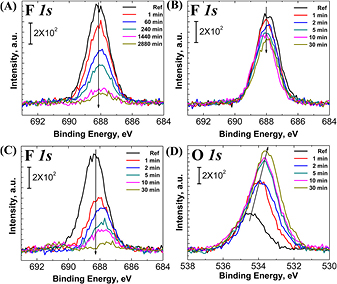
Figure 7. XPS F 1s core level spectra for a degreased Si3N4 sample etched for 4 min in 10% HF(aq), rinsed immediately with DI, dried under N2(g) and then followed by: (A) immersion in 23 °C DI water as a function of time; or (B) rinsed under flowing DI as a function of time; or (C) immersed in 70 °C DI as a function of time. The XPS F 1s peak integrated areas of (A), (B), and (C) are summarized in figure S2 (stacks.iop.org/JPhysCM/00/0000/mmedia). (D) XPS O 1s core level spectra for the same sample described in (C).
Download figure:
Standard image High-resolution imageThese results are supported by LEIS data showing that, after 30 min immersion in 70 °C DIW, there is complete removal of all surface F, with a concomitant increase in surface O content (see supporting information figure S3) (stacks.iop.org/JPhysCM/28/094014/mmedia).
Two possible mechanisms for fluorine removal are direct substitution of F by OH through reaction of H2O with Si–F as detailed in ref [36], or etching of silicon nitride. Etching can be easily measured by monitoring the phonon absorption of the Si3N4 films with IRAS. A series of IRAS measurements performed after immersion of HF-etched Si3N4 samples in 70 °C DI for increasing times are plotted in figure 8, which shows the high frequency range of OH stretch modes (3500–3900 cm−1; figure 8(A)) and the lower frequency range of nitride phonons (600–1500 cm−1; figure 8(B)). The spectrum (a) in figures 8(A) and (B) corresponds to degreased Si3N4 sample etched for 1 min in 1% HF(aq), immediately rinsed in DI, and dried under N2(g), referenced to the degreased Si3N4 sample prior to HF(aq) etching.
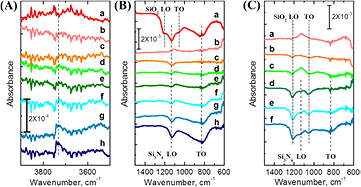
Figure 8. (A), (B) Infrared absorption spectra of (a) the degreased Si3N4 surface etched for 1 min in 1% HF(aq), immediately rinsed in DI, and dried under N2(g), then (b)–(h) immersed in 70 °C DI for (b) 1 min, (c) 5 min, (d) 10 min, (e) 30 min, (f) 60 min, (g) 120 min, and (h) 180 min, respectively. Spectrum (a) was referenced relative to the degreased Si3N4 surface prior to etching; spectra (b)–(h) were referenced relative to the HF-etched, DI rinsed, and dried surface to better highlight small chemical changes just due to the 70 °C DI immersion. (C) Infrared absorption spectra of a degreased but unetched Si3N4 surface immersed in 70 °C DI for the same times as in (A) and (B): (a) 1 min, (b) 5 min, (c) 10 min, (d) 30 min, (e) 60 min, and (f) 120 min, respectively. Spectra in (C) were referenced relative to the degreased Si3N4 surface.
Download figure:
Standard image High-resolution imageThe IRAS spectra (b-h) in figures 8(A) and (B) are all referenced relative to the HF(aq)-etched, DI rinsed, and N2(g) dried nitride surface to focus on the chemical changes due to subsequent immersion in 70 °C DI for various times. With this spectral reference, a flat line would indicate no change after water immersion. After 30 min of 70 °C DI immersion, the Si3N4 phonon modes are just starting to show some loss/disruption (figure 8(B) (e); dark green line), but the Si–OH peak is nearly as positive in magnitude as it was negative in magnitude after the HF etch (figure 8(A) (e); dark green line).
There is a clear loss of both the native SiO2 oxide (SiO2 TO and LO phonon modes at 1056 and 1200 cm−1) and Si3N4 phonons (Si3N4 TO and LO phonon modes at 827 and 1134 cm−1) consistent with etching. A weak loss at 3740 cm−1 corresponds to loss of OH on the initial degreased native-oxide-terminated Si3N4 sample, but it is very weak because there is also OH on the HF etched surface. Specifically, the native oxide surface is expected to be predominantly terminated with atop Si–OH sites, so the data of figure 8 indicate that the resulting HF(aq)-etched, DI rinsed, and N2(g) dried surface has fewer Si–OH sites, as expected from the formation of atop Si–F sites as observed by XPS and LEIS. The negative peak on figure 8(B) (a) does not imply that all Si–OH is removed during the HF etch, it merely implies that there are fewer Si–OH species on the etched nitride surface relative to the native oxidized surface.
We note that IRAS data cannot provide direct evidence for F termination as clearly as XPS and LEIS data shown in figures 2 and 3 because there is a strong change in the absorption of the Si3N4 transverse optical (TO) phonon mode, which exists in the same spectral region where the relatively weak Si–F modes (840 cm−1) are typically observed. In fact, the XPS and LEIS data in figures 7 and S3 (stacks.iop.org/JPhysCM/28/094014/mmedia) are essential to show that all Si–F sites are removed by this 70 °C DI treatment; the IRAS spectrum in figure 8(A) (e), which shows a nominally flat spectrum, implies that these Si–F sites are quantitatively replaced by Si–OH sites to achieve the same surficial Si–OH concentration as was evident on the native oxynitride surface.
Complementary AFM and contact angle measurements were performed to better characterize the surfaces after these various chemical treatments. The essential results are summarized in table 2. The main results from AFM are that surface roughness does not increase through the course of HF etching and that XPS, LEIS, and IRAS studies of the surface exposed to 30 min 70 °C DI immersion will not be complicated by increases in surface area. The water contact angle of 31° after degreasing the native oxide surface is consistent with a reasonably high Si–OH concentration. Upon HF etching, 1.3 nm of Si3N4 is etched (consistent with the phonon losses of figure 8(B), (a)) and the water contact angle increases to 40° due to the addition of hydrophobic Si–F sites (but does not increase more dramatically due to the residual presence of Si–OH and NH2 sites). Upon immersion of the etched sample in 70 °C DI for 30 min, the film thickness is not changed (consistent with the negligible phonon loss of figure 8(B), (e)), but due to the increase in Si–OH sites (figure 8(A), (e)) the water contact angle has decreased to 17°.
Table 2. Root-mean-square (RMS) surface roughness by AFM measured over 10 μm2 × 10 μm2, water contact angle by goniometry, and Si3N4 layer thickness determined by spectroscopic ellipsometry after as various surface chemical treatments.
| Sample number | Sample description | RMS (nm) | Contact angle (°) | Film thicknesses (nm) |
|---|---|---|---|---|
| 1 | Degreased native-oxide-terminated Si3N4 | 0.60 | 31 | 30.8 ± 0.1 |
| 2 | Degreased Si3N4 etched for 1 min in 1% HF(aq), immediately rinsed in DI, and N2(g) dried | 0.27 | 40 | 29.5 ± 0.1 |
| 3 | Sample 2, after 30 min in 70 °C DI | 0.31 | 17 | 29.4 ± 0.1 |
Therefore, for short immersion times in hot water (<30 min in 70 °C DI), the surficial Si–F sites could be replaced by Si–OH through a putative pentavalent Si transition state as demonstrated for the Si–F sites on atomically smooth Si(1 1 1) [35, 36], and summarized in scheme 2 [39–41].
Scheme 2. Proposed mechanism for removal of surficial Si–F upon exposure to 70 °C DI for 30 min [35, 36].
Download figure:
Standard image High-resolution imageFor longer immersion times in 70 °C DI, the HF-etched Si3N4 surface clearly exhibits Si3N4 phonon loss (figure 8(B), (f)–(h)) and continued increase in the Si–OH surface concentration (figure 8(A), (f)–(h)). As there is no increase in the phonon modes for SiO2 (or oxidized nitride) under these immersion conditions, the IRAS spectra are more consistent with Si3N4 material loss (etching) rather than mere conversion of Si3N4 to oxynitride. To a certain extent, it is surprising that the 70 °C DI treatment favored material etching over the growth of an oxidized overlayer. One possibility is that the 70 °C DI treatment can simultaneously oxidize Si3N4 and chemically etch the resulting oxide or oxynitride layer. To determine if an oxide/oxynitride layer can be removed under conditions of 70 °C DI immersion, a degreased native oxide-terminated Si3N4 was immersed in 70 °C DI for various times and monitored by IRAS (figure 8(C), (a)–(f)). The IRAS spectra show loss of SiO2 TO and LO phonon modes at 1056 and 1200 cm−1 for times up to 30 min followed by loss of Si3N4 TO and LO phonon modes at 827 and 1134 cm−1 for longer immersion times. These results indicate that, over long times, 70 °C DI water slowly etches both Si3N4 and oxynitride overlayers, presumably through hydrolyzation of both Si3N4 and oxidized nitride. While the intermediate steps likely involve oxidation of Si–N–Si backbonds, the hydrolyzation in general could be described as (Si3N4 + 12 H2O → 3Si(OH)4 + 4NH3) [42].
It is important to pause here for a moment to discuss some perspective regarding our choice to use the term 'etch'. While it is indeed an etch process that we are observing here, as evidenced by loss of both nitride and oxynitride bulk phonon modes, the etch rate is very slow. The amount of nitride phonon modes lost during the 120 min of 70 °C DI exposure (figure 8(B), (h)) is roughly similar in magnitude to those observed during a 1 min etch in 1% HF (figure 8(B), (a)). As the amount of material etched during the 1 min 1% HF process was measured to be 1.3 nm (table 2), this estimates the etch rate of Si3N4 in 70 °C DI to be (1–2) × 10–4 nm s−1. Obviously, this would not be considered a viable etch process if the goal was material removal, but from the perspective of understanding the stability of surface chemical species over the course of a modification reaction, it is critically important. It means water cannot be used as a solvent for Si3N4-selective surface reactions due to the formation of surficial Si–OH sites, which would therefore lose chemical specificity with the SiO2 surface.
3.2. Chemical functionalization of HF(aq)-etched Si3N4 films
In section 3.1, we provided evidence for the presence of F-, HO- and NH2-termination of HF(aq)-etched Si3N4 surfaces with quantification of the F coverage, but only rough estimates of OH and NH2 coverages. In this section, we use chemical grafting of specific molecules not only to test whether these groups are reactive and if selective functionalization is possible, but also to help quantify their coverage, starting with silanes (known to react with OH) and ending with aldehydes (known to attach to organic NH2 groups through Schiff-base reactions).
The previous sections showed that HF(aq)-etched Si3N4 surfaces are terminated with some surficial Si–OH sites. To estimate the Si–OH surface concentration and to test for any reactive selectivity to SiO2, HF(aq)-etched, DI rinsed, and N2(g) dried surfaces of Si3N4 and SiO2 were separately reacted with various organosilanes or organosiloxanes including octadecyltrichlorosilane (ODTCS), chlorodimethyloctadecylsilane (CDMODS), octadecytriethoxysilane (ODTES), and aminoundecyltriethoxysilane (AUTES) as shown in scheme 3. These molecules were chosen to test the different reactivity between the trichloro group and the triethoxylsilyl group [7, 43], and to titrate the SiOH surface coverage using a molecule (CDMODS) with only 1 reactive site; the tri-functional groups (ODTCS, ODTES, and AUTES) could polymerize off the surface in the presence of sufficient traces of water [6]. Therefore, to focus on the attachment to surface OH without potential for crosslinking, we started with a monochloro-organosilane (CDMODS) [5], characterized by the spectrum A in figure 9.

Figure 9. Transmission IR absorption spectra of (A) neat CDMODS, (B) CDMODS reacted with the HF(aq)-etched, DI rinsed, and N2(g) dried Si3N4 surface, (C) CDMODS reacted with a similarly prepared SiO2 surface. All spectra were referenced to the etched, rinsed, and dried spectrum obtained immediately prior to modification with SAM.
Download figure:
Standard image High-resolution image
Scheme 3. Structures of the alkylsiloxanes for chemical modification of the HF(aq)-etched, DI rinsed, and N2(g) dried Si3N4 and SiO2 surfaces.
Download figure:
Standard image High-resolution image3.2.1. Reaction of etched surfaces of Si3N4 or SiO2 surfaces with CDMODS.
For these experiments, a series of degreased Si3N4 samples were etched for 1 min in 1% HF(aq), rinsed immediately in DI, dried under N2(g), and then transferred to a dry box for reaction in a 1 mM toluene solution of CDMODS at 70 °C for 1 h. The loss of Si–OH (negative peak at 3680 cm−1) along with the formation of Si–O–Si (positive peaks at 1100 and 1020 cm−1), Si–CH3 (positive deformation mode at 1263 cm−1), and CHx (positive stretching modes between 2850–3000 cm−1) in the spectrum of figure 9(B) all point to a reaction between the SiOH sites of the etched nitride surface and chlorodimethyloctadecylsilane (CDMODS). There is no observable change in the IR absorption of the Si3N4 LO/ TO phonon modes region (800–1200 cm−1), which indicates that no etching occurred during the surface modification reaction in this nominally anhydrous environment. The peak area of the negative OH band (3600–3800 cm−1) on the nitride surface is 37% ± 16% of that observed for SiO2 surface; this means that the Si–OH content available for reaction with CDMODS on the etched, rinsed, and dried nitride surface is, similarly, 37% ± 16% of that available on the similarly prepared SiO2 surface. Interestingly, despite the difference in OH coverage, the integrated areas for the CHx stretching region of the CDMODS overlayer are similar: 0.0377 ± 0.0002 cm−1 for the nitride surface and 0.0364 ± 0.0002 cm−1 for the oxide surface (see section S1 in supplementary information for consideration of these estimates) (stacks.iop.org/JPhysCM/28/094014/mmedia). Also, the packing density of the CDMODS overlayer appears to be similar for both substrates, as evidenced by the same asymmetric methylene stretching frequency (2925 cm−1) for the CDMODS overlayer on both substrates; this stretching frequency corresponds to the densest layer achievable given the steric limitations of the dimethyl groups on the CDMODS silicon atom [44, 45].
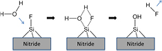
Since the monochlorosilane molecule does not have the capability to crosslink with neighboring molecules, every molecule must make a direct bond with the surface to be covalently bound. The discrepancy between loss of Si–OH and increase in hydrocarbon modes suggests that the CDMODS reacts with species other than the original number of Si–OH sites on the freshly etched, rinsed, and dried surface. The possibilities include (1) reaction of hydrolyzed CDMODS with a surficial Si–F site leading to F removal (scheme 4(A)), (2) conversion of surficial Si–F sites to Si–OH sites due to trace water impurities (F removal as shown in scheme 2), which can subsequently react with CDMODS (scheme 4(B)), and (3) reaction of the hydrolyzed CDMODS with Si–N–Si or Si–O–Si backbonds without F removal (scheme 4(C)). Keeping such possibilities in mind, the main conclusion of this section is that silane molecules can be grafted and completely cover HF(aq)-etched silicon nitride surfaces to same level as that achieved on a SiO2 surface.
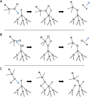
Scheme 4. Possible pathways for CDMODS to react with the HF(aq)-etched, DI rinsed, and dried Si3N4 surface. Here, and in other schemes, curved lines represent bonds to the rest of the Si3N4 bulk. (A) Reaction of hydrolyzed organosilane with surficial Si–F groups to eliminate HF. (B) Reaction of the chlorosilane at surficial Si–OH sites, which could either be the ones present on the surface immediately after HF(aq)-etching, DI rinsing, and drying or could be new Si–OH species formed by hydrolysis of Si–F, Si–O–Si, and/or Si–N–Si groups with trace water during the chlorosilane reaction. (C) Reaction of the hydrolyzed silane with backbond Si–N–Si groups. An analogous reaction with backbond Si–O–Si, not shown, is also possible to give SAM attachment and a surficial Si–OH group.
Download figure:
Standard image High-resolution image3.2.2. Characterization of surfaces after surface modification with alkylsiloxanes.
Options A and B in scheme 4 imply the loss of surficial Si–F species during the reaction with alkysilanes. In order to test this hypothesis, XPS spectra were collected before and after CDMODS reaction on the HF(aq)-etched, DI rinsed, and N2(g) dried Si3N4 surfaces (figure 10). Because the CDMODS layer is thin relative to the photoelectron escape depth, the F 1s and Si 2p signals are expected to have little screening, and in any case the same screening for both. The F/Si ratio after reaction with CDMODS is 85% ± 10% of the value measured immediately prior to reaction. Given that the initial surface coverage of Si–F was 72% ± 2% of a monolayer after etch, rinse, and dry, this loss in Si–F is equivalent to only 10% of a monolayer and is, therefore, not large enough to solely explain the similar SAM coverages of CDMODS on Si3N4 and SiO2. Consequently, we propose that some reactions as described by scheme

Figure 10. XPS F 1s core level of the 1% HF(aq)-etched, DI rinsed, and N2(g) dried Si3N4 surface (black line) and subsequent CDMODS modified surface (red line), plotted as the area ratio of F/Si.
Download figure:
Standard image High-resolution imageNext, we use LEIS to quantify the coverage of F and O before and after CDMODS treatment in a complementary way. Due to the strong interaction of ~KeV ions with the surface in LEIS, the densely packed molecular overlayer (SAM) on the CDMODS-reacted HF-etched Si3N4 surface essentially prevents most of the He + ions scattering from Si, F, and O ions to be detected (figure 11(a)). Therefore, we performed a series of thermal treatments to remove the chemisorbed CDMODS layer, monitoring the O, F and Si peaks. Upon subsequent UHV anneals for 1 min to sequentially higher temperatures of 100, 200, 300, 400, 500, 600, and 800 °C, the Si, F, and O signal intensities gradually increases with similar relative magnitudes up to 600 °C, as expected for the thermal decomposition of the organic overlayer (figures 11(b)–(g)). At the highest temperatures (800 °C), the fluorine peak on the CDMODS-terminated HF-etched Si3N4 sample is reduced due to thermal desorption (figure 11(g), consistent with the spectrum of the HF-etched Si3N4 sample of figures 3 and 4.
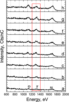
Figure 11. LEIS measurements of HF(aq)-etched, DI rinsed, and N2(g) dried Si3N4 after CDMODS reaction and after different LEIS UHV in situ 1 min thermal anneal conditions: (a) at 30 °C (no anneal) (b) 100 °C, (c) 200 °C, (d) 300 °C, (e) 400 °C, (f) 500 °C, (g) 600 °C, and (h) 800 °C, respectively. No sputtering of the surface was performed prior to analysis.
Download figure:
Standard image High-resolution imageA head-to-head comparison of F, O and Si signals is provided in figure 12: figure 12(a) (black line) represents the initial Si3N4 surface etched by 1% HF(aq) for 1 min, rinsed immediately in DI water for 30 s and dried under N2(g); figure 12(b) (green line) the Si3N4 surface etched by 1% HF(aq) for 1 min, rinsed immediately in DI water for 30s, dried under N2(g), and annealed at 600 °C; figure 12(c) (red line; same as figure 11(a)) the HF-etched, rinsed, dried, and CDMODS-terminated Si3N4 surface measured at 30 °C; and figure 12(d) (blue line; same as figure 11(g)) after annealing at 600 °C. Comparison of spectra d and b shows overall lower signal intensities of Si, F, and O for the functionalized surface after 600 °C; this is consistent with some decomposition residues (e.g. Si–O–Si(CH3)2–R) still being present on the surface and screening the O, Si, and F atoms. Nonetheless, despite this screening, the relative integrated areas of F/Si and F/O are 76% ± 11% and 63% ± 6% of the respective areas for the starting HF-etched surface. This 76% ± 11% retention of the starting Si–F after functionalization (and annealing) corroborates the XPS data in figure 11 (85% ± 10% retention of starting Si–F) and supports the model in which some Si–F moieties are consumed during organosilane reaction (see section S1 in supplementary information (stacks.iop.org/JPhysCM/28/094014/mmedia) for consideration of these estimates).

Figure 12. Comparison of LEIS spectra of (a) the Si3N4 surface etched by 1% HF(aq) for 1 min, rinsed in DI water for 30 s, and dried under N2(g) (black line), (b) the same surface as in (a) but annealed at 600 °C (green line), (c) the HF(aq)-etched, rinsed, dried, and CDMODS-reacted Si3N4 surface measured at 30 °C (red line), and (d) the HF(aq)-etched, rinsed, dried, and CDMODS-reacted Si3N4 surface after annealing at 600 °C (blue line). Note the reduced overall signal (for all: F, Si, O) and reduced F signal relative to Si on (d) relative to (b).
Download figure:
Standard image High-resolution image3.2.3. Examining selectivity with organosilanes: reaction of HF(aq)-etched surfaces of Si3N4 or SiO2 with other organosilanes.
Reaction of the HF(aq)-etched Si3N4 or SiO2 surfaces were performed with other organosilanes to ensure consistency with the results observed for CDMODS. IRAS spectra resulting from the ODTCS and ODTES reaction with HF(aq)-etched, DI rinsed, and N2(g) dried Si3N4 or SiO2 surfaces are presented in figures 13(A) and (B). Similar IRAS spectra for AUTES neat, and after reaction with HF(aq)-etched, DI rinsed, and N2(g) dried Si3N4 or SiO2 surfaces are shown in the supplementary information (figures S4 and S5) (stacks.iop.org/JPhysCM/28/094014/mmedia). In all cases, the results show similar trends with the results presented in section 3.2.1: higher loss in the Si–OH peak region between 3600–3800 cm−1 for the SiO2 substrates relative to the corresponding Si3N4 substrates, but similar intensities in the modes ascribed to the addition of the organic over layers. The intensities of these IR modes (~10−4) for all surfaces are consistent with monolayer coverage of SAM on surfaces (~2 × 10⁻⁴) [46, 47]. Consequently, none of the chloro- and ethoxy-silane molecules tested in this study showed any selectivity in reaction between Si3N4 and SiO2. Once formed, the SAM layers did not show any selectivity in subsequent etch removal as well, as detailed in supplementary information (section S2) (stacks.iop.org/JPhysCM/28/094014/mmedia).

Figure 13. Transmission IRAS absorption spectra of (A1) neat ODTCS, (A2) ODTCS reacted with the HF(aq)-etched, DI rinsed, and N2(g) dried Si3N4 surface, and (A3) ODTCS reacted on the similarly prepared SiO2 surface. IRAS absorption spectra for (B1) neat ODTES, (B2) ODTES reacted on HF(aq)-etched, DI rinsed, and N2(g) dried Si3N4 surface, and (B3) ODTES reacted on the similarly prepared SiO2 surface. All spectra were referenced to the corresponding etched, rinsed, and dried surface obtained before modification with SAM.
Download figure:
Standard image High-resolution image3.2.4. Schiff-base-style reaction with surficial –NH2 modes of the HF(aq)-etched Si3N4 surface and quantification of the surficial –NH2 concentration.
Due to their absence on similarly prepared SiO2 surfaces, the surficial Si–NH2 sites of the HF(aq)-etched, DI rinsed, and N2(g) dried Si3N4 films may present a route toward chemical selectivity between these two surfaces. We therefore turn to organic aldehydes that are known to react well with organic amines at low temperature [48–50]. Such Schiff-base-style reactions between aldehydes and the surficial Si–NH2 modes have been previously proposed [28], but evidence for a direct chemical reaction has not been conclusive. To test this mechanism, HF(aq)-etched, DI rinsed, and N2(g) dried Si3N4 wafers were immersed in 0.4 M undecanal (UDA) in dry methanol at 65 °C for 16 h, and the corresponding IRAS absorption spectrum is shown in figure 14(D). Evidence for reaction is shown by the loss of Si–NH2 modes at 3426 and 1550 cm−1, the gain of CHx modes at 1450 cm−1 (–CH2– deformation) and between 2800–3000 cm−1 (C–H stretching), and the gain of a mode at 1726 cm−1, which is assigned to the Si–N=C bond. While Schiff-base imine peaks for organic moieties (e.g. C–N=C) typically appear between 1690–1630 cm−1 [51], the higher frequency of the Si–N=C mode arises from the lower electronegativity of Si relative to C, which results in a stronger N=C bond due to its higher electron density. The static water contact angle increased from 40° ± 1° on the HF(aq)-etched, DI rinsed, and N2(g) dried Si3N4 surface to 80° ± 1° after the undecanal (UDA) reaction, consistent with molecular grafting. Because the WCA is lower than the >100° value typically observed for densely packed methyl-terminated monolayers [52], a further quantification of the surface coverage is desired

Figure 14. Differential infrared absorption spectra of (A) AUTES modified SiO2 surface versus piranha cleaned SiO2 surface, (B) SiO2-AUTES surface modified with UDA to form SiO2-AUTES-UDA versus piranha cleaned SiO2 surface, (C) SiO2-AUTES-UDA versus SiO2-AUTES surface, (D) UDA modified Si3N4 versus HF-etched Si3N4 surface.
Download figure:
Standard image High-resolution imageAs the oscillator strengths for the Si–N=C and C–N=C bonds are unknown, a direct quantification of the UDA coverage from IRAS and water contact angle is not possible. Our best estimate for the UDA coverage (and by inference the Si–NH2 coverage) is to compare the amount of UDA reacted on the HF(aq)-etched, water rinsed, and N2(g) dried Si3N4 surface to that reacted on a control SiO2-AUTES surface containing terminal –(CH2)11NH2 groups (see supplementary information section S3) (stacks.iop.org/JPhysCM/28/094014/mmedia). Figure 14(A) shows the IRAS spectrum of the AUTES layer relative to the cleaned SiO2 surface. The IRAS spectrum of the total SAM layer (AUTES + UDA) relative to the cleaned SiO2 surface is shown in figure 14(B), and only the spectroscopic changes observed upon UDA reaction are shown in figure 14(C); this latter spectrum is the best one used for comparison with the UDA-reacted Si3N4 surface (figure 14(D)). Consistent with a Schiff-base reaction on the control SiO2-AUTES surface, the amine vibration (C–NH2) at 1550 cm−1 (figure 14(A)) disappears in figure 14(B) (negative peak in figure 14(C)), an imine bond (C–N=C–C) appears at 1670 cm−1 (figures 14(B) and (C)), and an increase in the CHx stretching region (2800–3000 cm−1) occurs (figures 14(B) and (C)). Comparison of the integrated C–H stretching areas shows that the number of UDA molecules attached to the HF(aq)-etched, DI rinsed, and N2(g) dried Si3N4 surface is 17% ± 5% of that attached to the AUTES-SiO2 surface (see C–H stretching area details in table 3). Assuming that 100% of the Si–NH2 species on the Si3N4 surface reacted with UDA, that the number of C–NH2 sites on the AUTES-SiO2 surface represents 1 monolayer, and that no UDA molecules were physisorbed into/onto the AUTES-SiO2 SAM layer allows us to estimate the Si–NH2 coverage at a similar 17% ± 5%. While the estimate of Si–NH2 coverage could benefit from a more direct measurement, clearly the amount of UDA reaction on Si3N4 is not substantially large. The key question, however, is if this Si3N4-UDA SAM layer can sufficiently block subsequent chemical reactions to enable selective surface chemical modification. This is investigated in the next section.
Table 3. CH and C=N stretching region area on both SiO2 and Si3N4 surfaces.
| Surface | Area of CH stretching (cm−1) (2750–3050 cm−1) | Area of C=N stretching (cm−1) (1670–1727 cm−1) |
|---|---|---|
| SiO2-AUTES (a) | 0.193 ± 0.001 | — |
| SiO2-AUTES-UDA (b) | 0.354 ± 0.001 | — |
| Differential (b/a) | 0.216 ± 0.001 | 0.029 ± 0.005 |
| Si3N4-UDA | 0.037 ± 0.001 | 0.002 ± 0.001 |
3.2.5. Procedure for selective functionalization.
To investigate potential selective functionalization, UDA grafting on HF(aq)-etched, DI rinsed, and N2(g) dried SiO2 was examined. In contrast to the UDA reaction on a similarly prepared Si3N4 surfaces, the IRAS spectrum showed no evidence of UDA attachment on SiO2 after similar treatment (figure 15(A)), with no change in the low (33 ± 1°) static water contact angle. The results are graphically illustrated in scheme S2 (supplementary information) (stacks.iop.org/JPhysCM/28/094014/mmedia). Instead, as published previously [53], the spectral features in the SiO2 spectrum in figure 15(A) are consistent with reaction of surficial Si–OH sites with the methanol solvent to form SiOCH3 moieties: Si–OH loss at 3750 cm−1, SiO2 phonon losses at 1250 and 1000 cm−1, appearance of the complex O–CH3 mode (1105 cm−1), appearance of the OC–H3 deformation (1205 cm−1), and appearance of C–H stretching modes (2854, 2956, and 2992 cm−1). The absence of a UDA reaction on the SiO2 surface suggests that chemical selectivity between SiO2 and Si3N4 could be achieved if aldehyde-reacted Si3N4 surfaces do not subsequently react with silanes such as CDMODS, but the partially methanol-reacted SiO2 surfaces do.

Figure 15. IRAS spectra for (A) 1 min 1% HF(aq)-etched, DI rinsed, and N2(g) dried SiO2 and Si3N4 surfaces after reaction with the UDA/methanol solution. Evidence for bonding of UDA SAMs via Si–N=C– linkages are observed for the Si3N4 surface, while only methoxyl formation (and not UDA grafting) is observed on the SiO2 surface under the same reaction conditions. (B) The UDA/methanol treated surfaces from (A) after exposure to a CDMODS solution under the conditions describe in section 3.2.1; the UDA SAM layer prevents reaction of the CDMODS molecule from grafting onto the Si3N4 surface (the red differential FTIR spectrum is flat), while the methoxy terminated SiO2 surface still allows grafting of CDMODS. This chemical reaction scheme therefore exhibits selective chemical attachment: UDA grafting only on Si3N4 surface and CDMODS grafting only on the SiO2 surface.
Download figure:
Standard image High-resolution imageTo test this possibility for selective surface chemical reaction, we have reacted UDA-exposed samples of SiO2 and Si3N4 with CDMODS under the same conditions as described in section 3.2.1, and IRAS results are shown in figure 15. In contrast to the HF(aq)-etched, DI rinsed, and N2(g) dried Si3N4 surface, the UDA-terminated Si3N4 surface showed no reaction with CDMODS, i.e. the relatively low UDA SAM coverage (section 3.2.4) is apparently sufficient to prevent subsequent chemisorption by chlorosilanes. In contrast, a reaction with CDMODS was clearly observed on the corresponding SiO2 surface despite its partial surface methoxylation; evidence for the CDMODS reaction (figure 15(B), black line) is apparent from the appearance of C–H stretching modes (2860, 2927, and 2960 cm−1), Si–CH3 umbrella mode (1257 cm−1), and Si–O–Si bonds (1040 and 1100 cm−1). Integration of the spectral features of CDMODS (as described in section 3.2.1) shows that only 61% ± 8% of the SiO2 surface becomes CDMODS terminated (relative to the corresponding non-UDA-reacted SiO2 surface); the remaining surface fraction is assumed to be methoxyl terminated.
These results are significant because they provide a practical method to achieve selectivity of surface reaction on HF(aq)-etched SiO2 and Si3N4 surfaces. They also underscore the fact that complete surface termination is not critical for selectivity when relatively bulky organic molecules are used. These results provide the first clear proof-of-principle demonstration that selective chemical functionalization between silicon nitride and silicon dioxide is possible. The scheme presented here treats both surfaces to the exact same sequence of steps and processing conditions: HF(aq) etching, DI rinsing, N2(g) drying, reaction with UDA in methanol (where only the nitride surface becomes passivated with a UDA SAM), and subsequent reaction with chlorosilane in toluene (where only the oxide surface becomes passivated with the CDMODS SAM). The key to chemical selectivity stems from the ability to create unique chemical functionality between the two surfaces of interest and to arrange the reaction steps in the proper order. Note that selectivity would be lost if the CDMODS reaction were to run prior to the UDA reaction. In this case, it depends critically on the concentration of Si–NH2 that can be stabilized on the Si3N4 surface. To this end, a deeper understanding of the mechanisms associated with Si–NH2 generation during HF(aq) etching and their persistence through subsequent processing is critically important. Some insights into the formation and stability of Si–NH2 groups learned from this work are discussed in the final section 3.3.
3.3. Discussion of the etching mechanism and surface chemical composition of Si3N4 in HF(aq)
The HF-etched Si3N4 surfaces used in this work contain a mixture of chemically distinct species comprising Si–F (72% ± 2% of a ML), Si–OH (37% ± 16% of a ML), Si–NH2 (17% ± 5% of a ML), and subsurface Si–O bonds (see supplemental information section for a description of the error bars) (stacks.iop.org/JPhysCM/28/094014/mmedia). Below is a listing of our experimental results that, when evaluated in the context of other publications, illuminate some plausible mechanistic pathways for the stabilization of these chemical species on the surface:
- (1)Si–F is the dominant species at the surface. There is little, if any, subsurface F and there are no detectable N–F bonds.
- (2)The Si–F sites are stable to heat (up to 500 °C) and hydrolysis (hours are needed to remove the F in room temperature water).
- (3)The concentration of surficial Si–F does not depend on HF concentration, but the etch rate of the Si3N4 bulk does depend on HF concentration. This implies that a steady-state surface concentration of F exists during the etch process.
- (4)The concentration of surficial Si–OH or Si–NH2 is less than that of Si–F, and depends only weakly on HF concentration.
- (5)Small molecule aminosilane (Si–N containing) molecules are very hydrolytically sensitive and quickly react with ROH to form –NH + ROSi- molecules [54]. Despite this, there are still surficial Si–NH2 groups active enough to react with aldehydes but not to be hydrolyzed during the post-etch water rinsing steps.
- (6)Oxygen is present both at and below the surface.
- (7)There are no detectable surface reactive Si–H bonds under the reaction conditions tested in this work, but small levels of Si–H and Si–NH2 impurities are observed within the bulk of the Si3N4 films.
The simplest model that is consistent with all of these observations includes the generation of a steady-state distribution of surficial Si–F and Si–NH2 sites during HF(aq) etch [26] followed sequentially by Si–N hydrolysis, Si–OH formation, and backbond oxidation during water rinse. For dilute or buffered HF(aq) conditions both mechanisms could be acting concurrently. A key secondary parameter consistent with all of these observations is reaction control (of both etching and hydrolysis) imposed by surface steric strain. We elaborate further below.
Fluorine termination: scheme 5 combines the layer-by-layer etching steps previously published [26] into one scheme containing more total atoms but not showing the protonation expected for the N atoms in acidic etching solutions for clarity. It has been proposed [26] that the rate limiting step involves conversion of the surficial Si–NH2 site (scheme 5(A)) into a Si–F site (scheme 5(B)). While we propose below that a different rate-limiting step occurs for the overall etching of Si3N4, we do agree that conversion of Si–NH2 to the highly polarizing Si–F bond is critically important for activation of the Si–N backbonds to HF(aq) attack [36, 55, 56]. Due to this, the structure in scheme 5(G) is not expected to occur because it represents a reaction where the backbond Si–N sites are attacked by HF(aq) before the atop Si–NH2 site is converted to Si–F. Note that structure F (scheme 5) regenerates surficial Si–NH2 and Si–F sites similar to those in (A) and (B), respectively, such that the etching cycle continues until all Si3N4 material is removed. The choice of depicting the start of the etch cycle with the Si–NH2 species is therefore arbitrary, but helpful for the discussion above.
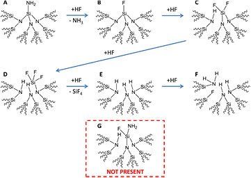
Scheme 5. Chemical structures expected to exist during the layer-by-layer etching of Si3N4 [26]. For simplicity of presentation, we are not showing all the possible charged species (e.g. Si– ,
,  , F−, etc), which although they can change the etch rate of Si3N4 do not appear to dramatically change the surface chemical composition (table 1). Similarly, the released NH3 and SiF4 species will quickly become
  and
and  when solvated in the HF(aq) solution. Under the low pH conditions of our HF(aq) etching solutions, we expect the N atoms of the structures shown here to be protonated in reality; this protonation will add additional steric strain relative to what is depicted here.
Download figure:
Standard image High-resolution imageWe now discuss what we believe to be the rate limiting step(s) for the overall Si3N4 etching mechanism. If the conversion of species A to B (scheme 5) were the rate limiting step as previously proposed [26], then the steady state surface concentration of Si–F would be very low, i.e. the surface would typically be Si–NH2 terminated. In contrast, we observe relatively high amounts of surficial Si–F sites independent of the HF(aq) concentration used. In fact, the experimentally observed Si–F content is expected to be the steady state Si–F content during etching because the hydrolysis of Si–F to Si–OH during the subsequent water rinse is practically negligible (figure 7(B)), which therefore reflects the true fluorine coverage in the etching solution. The rate limiting etch step(s) is(are) therefore better described by the reactions of C to D and/or D to E (scheme 5), because these structures have a relatively high surficial Si–F content. Note also that the surface concentrations of F, OH, and NH2 will sum to a total closer to 100% if the average atop silicon atom contains more than one F atom (vide supra). The surface species C and D (scheme 5) are the most sterically strained of the overall reaction especially when considering the additional protonation of nitrogen atoms expected for the low pH etching conditions of this work. Thus, we propose that the steric strain of species C and/or D slows Si-N backbond attack by HF(aq) such that these steps are the overall rate limiters for Si3N4 etching. Correspondingly, the HF etch rate has been shown to be dependent on the silicon nitride density (steric limitations) as well as HF concentration and pH (attack frequency and nitrogen/oxygen protonation) [57–59]. While this proposal is in contrast to the rate limiting steps proposed for the etching of SiO2 and Si, the uniquely high steady-state surface fluorine content of Si3N4 during HF etch warrants new consideration.
Presence of oxygen: scheme 5 does not, however, provide a complete picture of the whole etch process for Si3N4 as it does not include the formation of the experimentally confirmed oxygen-containing species. As discussed above, addition of oxygen through Si–F hydrolysis to Si–OH is not likely to occur during water rinse; and it is also not likely to occur during HF(aq) etching because rate for hydrolysis at 23 °C (figure 7(A)) is much lower than for etching (table 2). Hydrolyzation of the Si–N bonds could, however, lead to oxygen addition. The hydrolysis of Si–N bonds in molecular species such as hexamethyldisilizane (HMDS) is quite rapid for both water and silanol containing species [54]. It is therefore reasonable to expect that available Si–N bonds of the Si3N4 surface will be hydrolysed either during the post-etch water rinse and/or possibly during etch in very dilute HF(aq) or buffered HF(aq) solutions [18]. Scheme 6 shows a potential hydrolysis sequence for the Si–N bonds of the structure presented in scheme 5(C), which is one of the proposed steady-state etch species expected to be exposed during water rinse. Due to the pH increase during water rinse, de-protonation of the N atoms will occur during rinsing and this could reduce the steric strain of the surface enough to enable partial hydrolysis of Si–N backbonds during DI rinsing.

Scheme 6. Structures proposed for the hydrolysis of the steady-state species of scheme 5 C, which is reproduced here in structure (A). The high pH of the water rinse means that these schemes are expected to exist as drawn without the complication of N or O atom protonation; the lack of protonation makes room for water attack and hydrolysis of the Si–NH–Si bond shown in (A) to form neighbouring sites of Si–OH and Si–NH2 (B). Due to the steric strain of structure (B), complete hydrolysis to remove surface bound fluorine, as shown in structures (C)–(E), occurs for long times in either 70 °C or 23 °C water, or for long reaction times at 70 °C in the presence of trace water, but not during the 30 s post-etch water rinse (figure 7). A hydrolysis pathway allowing for more steric strain but still not F removal at 23 °C is shown in scheme S3 (supplementary information) (stacks.iop.org/JPhysCM/28/094014/mmedia).
Download figure:
Standard image High-resolution imagePresence of NH2: The experimental results (presence of F and some NH2) imply that backbone hydrolysis only occurs up to a certain point, e.g. at a structure similar to that described in scheme 6(B) or scheme S3(D) (supplementary information) (stacks.iop.org/JPhysCM/28/094014/mmedia). Data supporting the assignment of these surface species are: (1) water rinsing does not remove Si–F sites (scheme 6(E) not possible), (2) there are active Si–OH species after water rinse (scheme 6(A) not complete), (3) there are active Si–NH2 sites (schemes 6(A) and (E) not possible.) (4) there are no observable Si-NH-Si sites (schemes 6(A) and (C) not possible), and (5) there are fractionally more Si–F sites relative to Si–OH and Si–NH2 sites (scheme 6(B) preferred over 6(D)). It is curious that, despite the general hydrolytic activity of Si–NH2 sites, some of these groups still exist after water rinse.
To explain this, we invoke the argument of steric inhibition: the lower volume density Si–NH–Si modes (e.g. the left side of scheme 6(A)) will hydrolytically react with H2O to form the higher volume density combination of Si–OH and Si–NH2 (e.g. left side of scheme 6(B)). As the hydrolysis reactions of schemes 6 and S3 physically add more material to the surface, the local atomic density will increase up to a point where further hydrolysis reactions can no longer occur at an appreciable rate. Once this happens, the local region is under too much steric strain to allow the lone pair on an oxygen atom of an incoming H2O molecule to attack the Si atom of the Si–NH2 site; the N atom and two H atoms of the Si–NH2 site along with the neighboring Si–OH site (and other neighboring sites) block this Si atom from further hydrolytic attack.
Reaction of aldehydes (figure 15) on the sterically crowded Si–NH2 sites would still be possible, however, because it is the lone pair on the upper N atom of the Si–NH2 group that attacks the carbonyl carbon of the aldehyde to form the Schiff base imine product. So while steric limitations of the surface prevent the lower Si atom from further hydrolysis, the upper N atom is still available for subsequent reaction. Finally, the additional energy of the 70 °C water coupled with the 24 h reaction time seemingly allows the higher energy strain structures (schemes 6(C)–(E)) to proceed to fluorine removal (figure 7(D)) and Si3N4 etching (figure 8(C)).
Summary and outlook: The models presented here for etching and hydrolysis rely heavily on steric limitations but are fully consistent with the experimental results. Analogous to the self-limiting hydrolysis reactions proposed here, the silicon nitride material is known to grow a native oxide the depth of which depends on the material density [60]. As the Si3N4 used in this study is relatively dense, the native oxide thickness is only 1.3 nm after months of air exposure, and the hydrolysis of the Si–N backbonds during the DI rinse is expected to be limited to the very near surface region. Variations in material density could be one of the reasons for the seemingly contradictory reports on the surface chemical termination of nitride surfaces in the literature. In this light, a more detailed analysis of the surface chemical composition as a function of material density would be instructive. Careful molecular modelling of the steric energies of the structures (schemes 5, 6, and S3 (stacks.iop.org/JPhysCM/28/094014/mmedia), etc) proposed in this work would also be helpful for a more complete fundamental understanding of this work. The ability to selectively functionalize the silicon nitride surface is of high importance for the microelectronics industry. Unravelling the mechanisms underlying the formation of a robust chemical termination with Si–NH2 sites is therefore very important.
4. Conclusions
We have performed a relatively extensive analysis on the surface chemical composition and subsequent reactivity of the HF-etched high-density Si3N4 material. We have shown that the surface chemical composition is Si–F (70% ± 2% of a ML), Si–OH (37% ± 16% of a ML), Si–NH2 (17% ± 5% of a ML), and subsurface Si–O bonds. The F concentration on the surface is nominally independent of the concentration of HF(aq), but there appears to be slightly higher surface oxygen content and slightly lower surface nitrogen content with more dilute HF(aq). Due to the high steady-state surface fluorine content, we propose that the limiting step is the steric crowding at the surface required to remove SiF4. The surface-bound oxygen-containing species are most likely formed during the post-etch water rinse via hydrolysis of Si–N–Si backbonds, which appears to undergo full removal of surface fluorine and slow material etching at 70 °C. Selectivity in reaction between the HF-etched Si3N4 surface and the SiO2 surface was not achieved using reaction schemes involving Si–OH groups (as these are present on both surfaces), but rather by first employing a Schiff-base style reaction on surficial Si–NH2 groups unique to the nitride surface. An adsorbed undecyl SAM on the nitride surface is sufficient to prevent subsequent reaction with chlorosilane molecules that react selectively on the silicon oxide surface, thus resulting in selective functionalization. This initial work shows a clear first look at the surface chemistry involved in the challenging field of selective deposition.
Acknowledgments
This work was funded by Intel through the Semiconductor Research Corporation and the National Science Foundation (CHE 1300180). SP and HZ acknowledge NanoNextNL, a micro and nanotechnology consortium of the government of The Netherlands and 130 partners (program 6C) for funding.
TOC

Download figure:
Standard image High-resolution image